
Homework Answers
we can implement NOR gate using 2 pmos and 2 nmos.
in cmos circuit implementation of gates below network made by nmos gates should be the complement of the above network made by pmos gates.
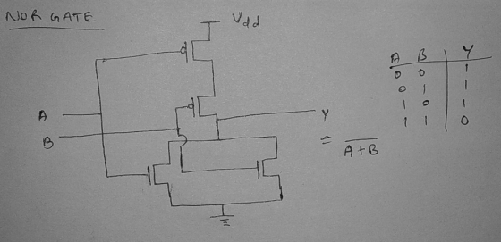
we will check for A = 1 and B = 1
both pmos off and both nmos on means output directly connected to ground means 0 as an output.
for physical circuitry we can use 5v as (1) and gnd as (0) for input.
please do not give thumbs down right away let me know in comment section if you don't understand it i will help.
Add Answer to:
4 CMOS FET Switches Design a NOR gate using only these 6 FET switches
Q.2) Using De Morgan's law: a) Design a 3-input NOR gate using 2-input NOR gate only....
 Q.2) Using De Morgan's law: a) Design a 3-input NOR gate using 2-input NOR gate only. Draw you diagram b) Design 4 input AND gate using 2 input NOR gates. Draw you diagram
In a CMOS NOR gate, if only one PMOS is ON, the output is ___. low...
In a CMOS NOR gate, if only one PMOS is ON, the output is ___. low voltage (logic zero) high voltage (logic high) depends on the state of NMOS none of the other choices
Arrange and sketch a CMOS circuit to form an NAND NOR and Not gate.
 Arrange and sketch a CMOS circuit to form an NAND NOR and Not gate.
Q1: Design Two-Input NAND Using NOR Gate(s) Creaete the NAND gate as specified in the following...
Q1: Design Two-Input NAND Using NOR Gate(s) Creaete the NAND gate as specified in the following instructions. * Truth table *Derive the NOR gate circuit using Boolean Algebra (I am not sure how to do this step, thanks) * Create the Circuit Q2: Design Two-Input NOR Using NAND Gate(s) Creete the NOR gate as specified in the following instructions. * Truth table * Derive the NOR gate circuit using Boolean Algebra * Create the Circuit
3. Design of a 2 input XNOR gate using CMOS transistors, a. Realize the 2 input...
 3. Design of a 2 input XNOR gate using CMOS transistors, a. Realize the 2 input XNOR gate using static CMOS transistor with truth table and necessary equation. (25 Marks) (20 Marks) b. Draw the stick diagram of 2 input XNOR gate; c.Apprpriate device sizing can result in equal and symmetrical drive current which leads to a sunstainable design. In order to obtained optimum operation of the cirut determine the(Whpe and (W/L) for the 2 input XNOR gate. Assume that...
Design a 2 input CMOS XNOR gate and submit the following: - CMOS diagram - Extended...
Design a 2 input CMOS XNOR gate and submit the following: - CMOS diagram - Extended truth table
Design a gate (ab + cd +e)' in CMOS technology using 5 nMOS and 5 pMOS...
Design a gate (ab + cd +e)' in CMOS technology using 5 nMOS and 5 pMOS transistors. Operator ' denoted complementation.
Design a 3 Input CMOS NAND gate. Please submit the following: - CMOS Diagram - Extended...
Design a 3 Input CMOS NAND gate. Please submit the following: - CMOS Diagram - Extended Truth Table - Stick Diagram (2 ways of designing it)
I am trying to find out a design containing NOR and OR or AND gate for the interface block design...
 I am trying to find out a
design containing NOR and OR or AND gate for the interface block
design. I have completed a design for when A = B, but I am having
difficulty designing A < B and B > A on the subtractor where
the boxes have question marks. Please help!
8.3* The circuit of 8.2, configured as a subtractor, can be used to compare two 4-bit numbers. Subtractor outputs C4 and (S3..S0) can be combined logically...
I am trying to find out a
design containing NOR and OR or AND gate for the interface block
design. I have completed a design for when A = B, but I am having
difficulty designing A < B and B > A on the subtractor where
the boxes have question marks. Please help!
8.3* The circuit of 8.2, configured as a subtractor, can be used to compare two 4-bit numbers. Subtractor outputs C4 and (S3..S0) can be combined logically...
solve 1 to 4 DEMUX by using cmos and draow the lgic gate by using nand
solve 1 to 4 DEMUX by using cmos and draow the lgic gate by using nand
 Q.2) Using De Morgan's law: a) Design a 3-input NOR gate using 2-input NOR gate only. Draw you diagram b) Design 4 input AND gate using 2 input NOR gates. Draw you diagram
 Arrange and sketch a CMOS circuit to form an NAND NOR and Not gate.
 3. Design of a 2 input XNOR gate using CMOS transistors, a. Realize the 2 input XNOR gate using static CMOS transistor with truth table and necessary equation. (25 Marks) (20 Marks) b. Draw the stick diagram of 2 input XNOR gate; c.Apprpriate device sizing can result in equal and symmetrical drive current which leads to a sunstainable design. In order to obtained optimum operation of the cirut determine the(Whpe and (W/L) for the 2 input XNOR gate. Assume that...
 I am trying to find out a
design containing NOR and OR or AND gate for the interface block
design. I have completed a design for when A = B, but I am having
difficulty designing A < B and B > A on the subtractor where
the boxes have question marks. Please help!
8.3* The circuit of 8.2, configured as a subtractor, can be used to compare two 4-bit numbers. Subtractor outputs C4 and (S3..S0) can be combined logically...
I am trying to find out a
design containing NOR and OR or AND gate for the interface block
design. I have completed a design for when A = B, but I am having
difficulty designing A < B and B > A on the subtractor where
the boxes have question marks. Please help!
8.3* The circuit of 8.2, configured as a subtractor, can be used to compare two 4-bit numbers. Subtractor outputs C4 and (S3..S0) can be combined logically...
Most questions answered within 3 hours.
-
A lottery exists where balls numbered 1 to 17 are placed in an
urn. To win,...
asked 3 seconds ago -
26) Briefly describe, using words or simple diagrams, the
chemiosmotic theory for coupling oxidation to phosphorylation...
asked 1 hour ago -
Suppose that XX is a random variable with mean 16 and standard
deviation 5 . Also...
asked 2 hours ago -
Calculate the number density of argon gas at a temperature of
24C and a pressure of...
asked 5 hours ago -
Alternative
Classification
How to Estimate
Probabilities from Data? ( For continuous Attributes)
And How to generate...
asked 5 hours ago -
An explosion breaks a 20.0-kg object into three parts. The
object is initially moving at a...
asked 6 hours ago -
Calculate the approximate number of residues of Rubisco, which
is involved in carbon fixation in plants,...
asked 7 hours ago -
Other decisions about scientific claims can have a much broader
impact.ENERGYarrow-10x10.png, environment, health, security - all...
asked 8 hours ago -
I need to write a research paper and work cited about this
topic: The United States...
asked 9 hours ago -
Hello! I was wondering if I could have some help?
If the vapor pressure of carvone...
asked 9 hours ago -
An economist wants to estimate the mean per capita income (in
thousands of dollars) for a...
asked 9 hours ago -
What would be the input/output characteristic of a circuit
obtained by putting two of your 2's-complementers...
asked 9 hours ago