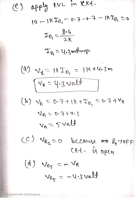
For the circuit in Figure 1, determine: a) VX, b) VA, c) VR2, d) VD5, and e) ID1. Consider the diodes to be Silicon (Si).

Homework Answers

Add Answer to:
For the circuit in Figure 1, determine: a) VX, b) VA, c) VR2, d)
VD5, and...
[2.5 marks] Design a combinational circuit (using two 8-to-1 multiplexers) with three inputs, and...
 [2.5 marks] Design a combinational circuit (using two 8-to-1 multiplexers) with three inputs, and one output to implement the following function. 10 12 13 14 Note: the answ er will be shown hand written on the same figures in the next page No need for EWE D3 VCC D2 D4 D1 DS DO D6 D3 VCC D2 D4 D1 D5 DO D6 GND C GND C 74151 74151
[2.5 marks] Design a combinational circuit (using two 8-to-1 multiplexers) with three...
[2.5 marks] Design a combinational circuit (using two 8-to-1 multiplexers) with three inputs, and one output to implement the following function. 10 12 13 14 Note: the answ er will be shown hand written on the same figures in the next page No need for EWE D3 VCC D2 D4 D1 DS DO D6 D3 VCC D2 D4 D1 D5 DO D6 GND C GND C 74151 74151
[2.5 marks] Design a combinational circuit (using two 8-to-1 multiplexers) with three...
Please answer clearly Determine voltage characteristics (Vout/V) of the circuit shown in Figure 1. Assume: a)...
 Please answer clearly
Determine voltage characteristics (Vout/V) of the circuit shown in Figure 1. Assume: a) Diodes D1 and D2 are ideal. b) Zener diode has r2-0 with the break down voltage of Vz-12 V. 1ΚΩ D1 D2 추 R2 1ΚΩ Vout Figure 1
Please answer clearly
Determine voltage characteristics (Vout/V) of the circuit shown in Figure 1. Assume: a) Diodes D1 and D2 are ideal. b) Zener diode has r2-0 with the break down voltage of Vz-12 V. 1ΚΩ D1 D2 추 R2 1ΚΩ Vout Figure 1
Q1. i) Will the current flow from A to C, for the connection shown in Figure....
 Q1. i) Will the current flow from A to C, for the connection shown in Figure. 12 Support your answer (11 with proper reasons. Both D1 and D2 are silicon diodes. D1 D2 A_* B Figure 1 ii) Draw the equivalent circuit diagram for Ideal Diode under forward bias and reverse bias. iii) Determine the value of I for the circuit shown in Figure. 2 R - 5V 15.2 V 5 kΩ Ge Figure 2 iv) Compute Vo and Ir...
In the circuit below, T1 is rated 12V RMS secondary voltage, D1, D2, D3 &D4 are IN4001 rectifying diodes and RL...
 In the circuit below, T1 is rated 12V RMS secondary voltage, D1, D2, D3 &D4 are IN4001 rectifying diodes and RL is 1.8ΚΩ. Given that RI-2202, and R2 1.2KQ, use the formula provided to calculate the output voltage (Vo) of the LM317 voltage regulator. Provide an answer in engineering notation, correct to 3 significant figures. 1 A Vo= 1.25V (1 + R2/ R1) Da AC line C CT input 60 Hz NC D, CI 120 V/12 V R2
In the...
In the circuit below, T1 is rated 12V RMS secondary voltage, D1, D2, D3 &D4 are IN4001 rectifying diodes and RL is 1.8ΚΩ. Given that RI-2202, and R2 1.2KQ, use the formula provided to calculate the output voltage (Vo) of the LM317 voltage regulator. Provide an answer in engineering notation, correct to 3 significant figures. 1 A Vo= 1.25V (1 + R2/ R1) Da AC line C CT input 60 Hz NC D, CI 120 V/12 V R2
In the...
ELTR 197 Analog Determine whether each silicon diode is forward or reverse biased. a) 1. b)...
 ELTR 197 Analog Determine whether each silicon diode is forward or reverse biased. a) 1. b) 10ka 100V B) Forward Bia sE OForwod Biase 5600 5V 8V d) 10KO 10ka 1.0kn $1.5kn -20V 10V -30V 4.7ka 4.7kQ 2. Using the practical diode model, determine the values of VR1, Vr2, and Vo. Vo R1 4 k7 D1 hika 22KS) R2 10V Via- 5V 13 -n the forward current of a diode with 1. Determine whether each silicon diode is forward or...
Consider the two-sided limiter circuit below. Let the load resistor RLoad = 1 kQ. The gain...
 Consider the two-sided limiter circuit below. Let the load resistor RLoad = 1 kQ. The gain must be 0.8 V/V in the region where the diodes are not limiting. Use a constant voltage drop model for the diodes with VD = 0.7 V. 3. out D2 (1+2 pts) Find the value for voltage source V1 that causes D1 to start limiting the output voltage at -5 V. a. D3 D1 Vin R2 b. (1+2 pts) Find the value for voltage...
(b) Figure Q5(b) shows a rectifier circuit topology that is used for single-phase power factor co...
 (b) Figure Q5(b) shows a rectifier circuit topology that is used for single-phase power factor correction. Sketch another topology that can be used for the same purpose and briefly describe how the topology operates D1 D3 L1 DS DC CBUL TR1 D2 D4 Fig. Q5(b) 6 marks
(b) Figure Q5(b) shows a rectifier circuit topology that is used for single-phase power factor correction. Sketch another topology that can be used for the same purpose and briefly describe how the topology...
(b) Figure Q5(b) shows a rectifier circuit topology that is used for single-phase power factor correction. Sketch another topology that can be used for the same purpose and briefly describe how the topology operates D1 D3 L1 DS DC CBUL TR1 D2 D4 Fig. Q5(b) 6 marks
(b) Figure Q5(b) shows a rectifier circuit topology that is used for single-phase power factor correction. Sketch another topology that can be used for the same purpose and briefly describe how the topology...
Please answer clearly 2. Consider the circuit shown in Figure 1. Determine values of Ri, R2, and Rc to provide the quie...
 Please answer clearly
2. Consider the circuit shown in Figure 1. Determine values of Ri, R2, and Rc to provide the quiescent emitter current 1.5 mA and the quiescent collector to emitter voltage 5V. Assume β 100, Re-I㏀、Va= 200V, VBEon-0.7V, and VT= 25mV. R1 Rc Vcc に 10v R2 Re Figure 1: BJT biasing configuration
2. Consider the circuit shown in Figure 1. Determine values of Ri, R2, and Rc to provide the quiescent emitter current 1.5 mA and the...
Please answer clearly
2. Consider the circuit shown in Figure 1. Determine values of Ri, R2, and Rc to provide the quiescent emitter current 1.5 mA and the quiescent collector to emitter voltage 5V. Assume β 100, Re-I㏀、Va= 200V, VBEon-0.7V, and VT= 25mV. R1 Rc Vcc に 10v R2 Re Figure 1: BJT biasing configuration
2. Consider the circuit shown in Figure 1. Determine values of Ri, R2, and Rc to provide the quiescent emitter current 1.5 mA and the...
Consider the oscillator circuit shown below. The op amp i s ideal Rb Vo R2 = 10 kΩ L2 100 mH R1 1...
 Consider the oscillator circuit shown below. The op amp i s ideal Rb Vo R2 = 10 kΩ L2 100 mH R1 1 k2 L1 = 10 mH a. What is the frequency of oscillation in Hz? b. Specify the required value of Rb sustain oscillations. c. A limiter circuit is added to oscillator by separating Rb into two series resistors Rb1 and Rb2 as shown in the next page along with two anti-parallel diodes in shunt with Rb2. determine...
Consider the circuit shown in Figure 1. Assume that the diodes have an exponen Question 21 tial i-v characteristic....
 Consider the circuit shown in Figure 1. Assume that the diodes have an exponen Question 21 tial i-v characteristic. Diode D1 has 10 times the junction area of D2, i.e. Isı = 10Is2. Determine the value of voltage V indicated in the figure. The circuit operates at room temperature, i.e. the value of the thermal voltage is Vr = 26 mV 10 mA 3 mA Fig. 1 O+V
Consider the circuit shown in Figure 1. Assume that the diodes have...
Consider the circuit shown in Figure 1. Assume that the diodes have an exponen Question 21 tial i-v characteristic. Diode D1 has 10 times the junction area of D2, i.e. Isı = 10Is2. Determine the value of voltage V indicated in the figure. The circuit operates at room temperature, i.e. the value of the thermal voltage is Vr = 26 mV 10 mA 3 mA Fig. 1 O+V
Consider the circuit shown in Figure 1. Assume that the diodes have...
 [2.5 marks] Design a combinational circuit (using two 8-to-1 multiplexers) with three inputs, and one output to implement the following function. 10 12 13 14 Note: the answ er will be shown hand written on the same figures in the next page No need for EWE D3 VCC D2 D4 D1 DS DO D6 D3 VCC D2 D4 D1 D5 DO D6 GND C GND C 74151 74151
[2.5 marks] Design a combinational circuit (using two 8-to-1 multiplexers) with three...
[2.5 marks] Design a combinational circuit (using two 8-to-1 multiplexers) with three inputs, and one output to implement the following function. 10 12 13 14 Note: the answ er will be shown hand written on the same figures in the next page No need for EWE D3 VCC D2 D4 D1 DS DO D6 D3 VCC D2 D4 D1 D5 DO D6 GND C GND C 74151 74151
[2.5 marks] Design a combinational circuit (using two 8-to-1 multiplexers) with three...
 Please answer clearly
Determine voltage characteristics (Vout/V) of the circuit shown in Figure 1. Assume: a) Diodes D1 and D2 are ideal. b) Zener diode has r2-0 with the break down voltage of Vz-12 V. 1ΚΩ D1 D2 추 R2 1ΚΩ Vout Figure 1
Please answer clearly
Determine voltage characteristics (Vout/V) of the circuit shown in Figure 1. Assume: a) Diodes D1 and D2 are ideal. b) Zener diode has r2-0 with the break down voltage of Vz-12 V. 1ΚΩ D1 D2 추 R2 1ΚΩ Vout Figure 1
 Q1. i) Will the current flow from A to C, for the connection shown in Figure. 12 Support your answer (11 with proper reasons. Both D1 and D2 are silicon diodes. D1 D2 A_* B Figure 1 ii) Draw the equivalent circuit diagram for Ideal Diode under forward bias and reverse bias. iii) Determine the value of I for the circuit shown in Figure. 2 R - 5V 15.2 V 5 kΩ Ge Figure 2 iv) Compute Vo and Ir...
 In the circuit below, T1 is rated 12V RMS secondary voltage, D1, D2, D3 &D4 are IN4001 rectifying diodes and RL is 1.8ΚΩ. Given that RI-2202, and R2 1.2KQ, use the formula provided to calculate the output voltage (Vo) of the LM317 voltage regulator. Provide an answer in engineering notation, correct to 3 significant figures. 1 A Vo= 1.25V (1 + R2/ R1) Da AC line C CT input 60 Hz NC D, CI 120 V/12 V R2
In the...
In the circuit below, T1 is rated 12V RMS secondary voltage, D1, D2, D3 &D4 are IN4001 rectifying diodes and RL is 1.8ΚΩ. Given that RI-2202, and R2 1.2KQ, use the formula provided to calculate the output voltage (Vo) of the LM317 voltage regulator. Provide an answer in engineering notation, correct to 3 significant figures. 1 A Vo= 1.25V (1 + R2/ R1) Da AC line C CT input 60 Hz NC D, CI 120 V/12 V R2
In the...
 ELTR 197 Analog Determine whether each silicon diode is forward or reverse biased. a) 1. b) 10ka 100V B) Forward Bia sE OForwod Biase 5600 5V 8V d) 10KO 10ka 1.0kn $1.5kn -20V 10V -30V 4.7ka 4.7kQ 2. Using the practical diode model, determine the values of VR1, Vr2, and Vo. Vo R1 4 k7 D1 hika 22KS) R2 10V Via- 5V 13 -n the forward current of a diode with 1. Determine whether each silicon diode is forward or...
 Consider the two-sided limiter circuit below. Let the load resistor RLoad = 1 kQ. The gain must be 0.8 V/V in the region where the diodes are not limiting. Use a constant voltage drop model for the diodes with VD = 0.7 V. 3. out D2 (1+2 pts) Find the value for voltage source V1 that causes D1 to start limiting the output voltage at -5 V. a. D3 D1 Vin R2 b. (1+2 pts) Find the value for voltage...
 (b) Figure Q5(b) shows a rectifier circuit topology that is used for single-phase power factor correction. Sketch another topology that can be used for the same purpose and briefly describe how the topology operates D1 D3 L1 DS DC CBUL TR1 D2 D4 Fig. Q5(b) 6 marks
(b) Figure Q5(b) shows a rectifier circuit topology that is used for single-phase power factor correction. Sketch another topology that can be used for the same purpose and briefly describe how the topology...
(b) Figure Q5(b) shows a rectifier circuit topology that is used for single-phase power factor correction. Sketch another topology that can be used for the same purpose and briefly describe how the topology operates D1 D3 L1 DS DC CBUL TR1 D2 D4 Fig. Q5(b) 6 marks
(b) Figure Q5(b) shows a rectifier circuit topology that is used for single-phase power factor correction. Sketch another topology that can be used for the same purpose and briefly describe how the topology...
 Please answer clearly
2. Consider the circuit shown in Figure 1. Determine values of Ri, R2, and Rc to provide the quiescent emitter current 1.5 mA and the quiescent collector to emitter voltage 5V. Assume β 100, Re-I㏀、Va= 200V, VBEon-0.7V, and VT= 25mV. R1 Rc Vcc に 10v R2 Re Figure 1: BJT biasing configuration
2. Consider the circuit shown in Figure 1. Determine values of Ri, R2, and Rc to provide the quiescent emitter current 1.5 mA and the...
Please answer clearly
2. Consider the circuit shown in Figure 1. Determine values of Ri, R2, and Rc to provide the quiescent emitter current 1.5 mA and the quiescent collector to emitter voltage 5V. Assume β 100, Re-I㏀、Va= 200V, VBEon-0.7V, and VT= 25mV. R1 Rc Vcc に 10v R2 Re Figure 1: BJT biasing configuration
2. Consider the circuit shown in Figure 1. Determine values of Ri, R2, and Rc to provide the quiescent emitter current 1.5 mA and the...
 Consider the oscillator circuit shown below. The op amp i s ideal Rb Vo R2 = 10 kΩ L2 100 mH R1 1 k2 L1 = 10 mH a. What is the frequency of oscillation in Hz? b. Specify the required value of Rb sustain oscillations. c. A limiter circuit is added to oscillator by separating Rb into two series resistors Rb1 and Rb2 as shown in the next page along with two anti-parallel diodes in shunt with Rb2. determine...
 Consider the circuit shown in Figure 1. Assume that the diodes have an exponen Question 21 tial i-v characteristic. Diode D1 has 10 times the junction area of D2, i.e. Isı = 10Is2. Determine the value of voltage V indicated in the figure. The circuit operates at room temperature, i.e. the value of the thermal voltage is Vr = 26 mV 10 mA 3 mA Fig. 1 O+V
Consider the circuit shown in Figure 1. Assume that the diodes have...
Consider the circuit shown in Figure 1. Assume that the diodes have an exponen Question 21 tial i-v characteristic. Diode D1 has 10 times the junction area of D2, i.e. Isı = 10Is2. Determine the value of voltage V indicated in the figure. The circuit operates at room temperature, i.e. the value of the thermal voltage is Vr = 26 mV 10 mA 3 mA Fig. 1 O+V
Consider the circuit shown in Figure 1. Assume that the diodes have...
Most questions answered within 3 hours.
-
Consider a 3m x 3m window in a house. The thermal conductivity
is reported to be...
asked 9 minutes ago -
Why has California been the favorite destination of large number
of secondary migrants?
asked 43 minutes ago -
Do not neglect the old for the new. The existing business must
not lose priority simply...
asked 3 hours ago -
Kylie is a single mom with two dependent children,
Tanner, age 7 and Olivia, age 11....
asked 5 hours ago -
Phosphorous + bromine = phosphorous tribromide. If 35.0 g of
bromine are reacted and 27.9 grams...
asked 6 hours ago -
Derive the long wavelength limit of the Planck energy density
distribution
asked 6 hours ago -
Calculate the pH of each of the following solutions.
0.50 M HBr
3.1×10⁻⁴ M KOH
4.2×10⁻⁵...
asked 9 hours ago -
For the year ended December 31, Depot Max’s cost of merchandise
sold was $85,600. Inventory at the...
asked 9 hours ago -
Week 10 - Professional Memo Assignment
Professional Memo Assignment
Your mission for this week, should you...
asked 10 hours ago -
Write a Python program that stores the data for each
player on the team, and it...
asked 10 hours ago -
In
the last 3 months, mike never knows when he is going to get his
allowance...
asked 10 hours ago -
Is Ca(OH)2 a Bronsted base, Lewis base, or both? Why?
asked 10 hours ago