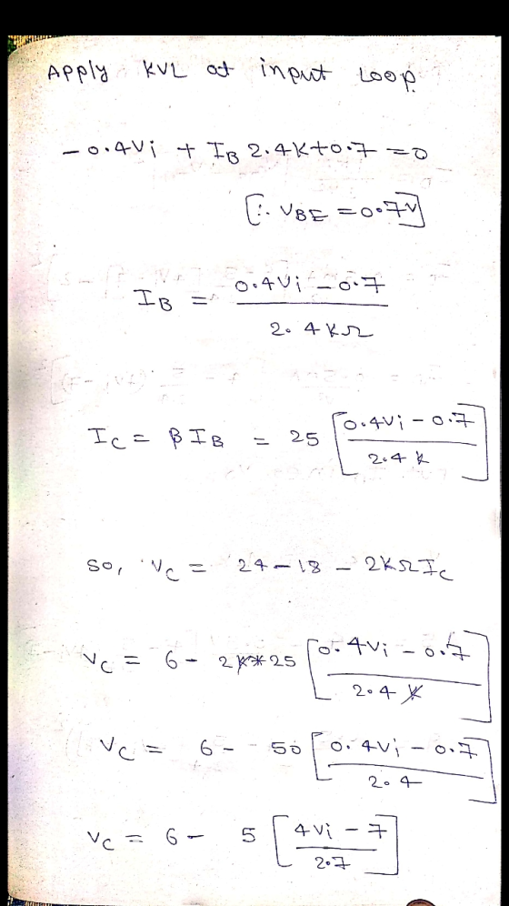
In the circuit of the figure, the bipolar transistor has a B = 25 and the MOSFET has a VTN = 2V as well as a conduction parameter Kn = 1mA / V ^ 2. Determine the value of the input voltage required for the output voltage Vo = 15V.

Homework Answers


![put ve in equation ID Io = IMA (Vgs - YTN]² 22 Is = O.S.MA V2 1.6 - 5 [Wi-7] -2) 2.4 ID 0.5mA V2, [+ (Avi-7) 2.4 put. Is in e](http://img.homeworklib.com/questions/0efb66e0-e5a3-11ea-9c52-3d4fac9ac0c4.png?x-oss-process=image/resize,w_560)
![2 18= Festa Cav; --2] - > 4:24 - 4 5 [avi-7 2-4 = ) 0:24 - 5 [avi z 2 0.116 - Avit7. V Avi 0012-7 tavia t 6.88 Vi = lo 72V Re](http://img.homeworklib.com/questions/0fcd0da0-e5a3-11ea-a965-cf41cbe2a0d4.png?x-oss-process=image/resize,w_560)
Add Answer to:
In the circuit of the figure, the bipolar transistor has a B =
25 and the...
Part "c" Please! Consider the circuit below. Assume that the only inductance of interest is the...
 Part "c" Please!
Consider the circuit below. Assume that the only inductance of interest is the load inductor L = 15mH connected to the output terminal. The resistors have the following values: R1 = 5kN, R2 = 2kN, R3 = 0.1kN, and RI, = 10kN. The supply voltage is Vs = 15V. Vs R2 R, vo R1 R3 Figure 6-1 It is known that the input voltage vị can be decomposed into two parts, a constant Vị and a small...
Part "c" Please!
Consider the circuit below. Assume that the only inductance of interest is the load inductor L = 15mH connected to the output terminal. The resistors have the following values: R1 = 5kN, R2 = 2kN, R3 = 0.1kN, and RI, = 10kN. The supply voltage is Vs = 15V. Vs R2 R, vo R1 R3 Figure 6-1 It is known that the input voltage vị can be decomposed into two parts, a constant Vị and a small...
All letters please . In the circuit below, the NMOS transistor has the threshold voltage of...
 All letters please
. In the circuit below, the NMOS transistor has the threshold voltage of V-0.5V.Assume that the MOSFET parameter VA-1/A-40V, operating at the drain voltage VD-2V. (10%) 30 RG vo l0kn a. what region is the transistor operating in? (10%) b. What is the value ofgm? (10%) c. What is the voltage gain vom? (10%)
All letters please
. In the circuit below, the NMOS transistor has the threshold voltage of V-0.5V.Assume that the MOSFET parameter VA-1/A-40V, operating at the drain voltage VD-2V. (10%) 30 RG vo l0kn a. what region is the transistor operating in? (10%) b. What is the value ofgm? (10%) c. What is the voltage gain vom? (10%)
Score 2. (22 points) For the circuit in Figure 2, the transistor parameters are: 2 0,...
 Score 2. (22 points) For the circuit in Figure 2, the transistor parameters are: 2 0, VN=2V, Ka-1mA/V2, all the capacitors are assumed to act as short circuits at the signal frequency (1) Calculate the Q-point (Vos. I Vos); (2) Sketch the small-signal equivalent circuit, you must label the polarities of the voltages and the direction of the current; (3) Determine the voltage gain A, vo/v (4) Determine the input resistance Ri and output resistance Ro V1 5 10 V...
Consider the following circuit. Assume that the transistor is in saturation with Vds = 2V. Further...
 Consider the following circuit. Assume that the transistor is in saturation with Vds = 2V. Further a.sume that kn = 4mA/V and VTN = 1V. Determine ID, Vo and Vin. 5V T 4.6K Vo Vin 1.4K
Figure 3 Transistor amplifire circuit with source Vs and load R b) For the BJT switching...
 Figure 3 Transistor amplifire circuit with source Vs and load R b) For the BJT switching circuit shown in Figure 4, i) Calculate the value of Ra so that the transistor is operating in saturation when switched on if the value of Rc is 3.9 kn. ii) What will the output voltage be for the applied input signal voltage shown if Vcet IS 0.2V? 5 V Re o V 5 V B 100 OV Figure 4 BUT switching circuit with...
Q5 Figure 4 is a common-source circuit. The PMOS transistor parameters are VTP = -0.6V, Kp...
 Q5 Figure 4 is a common-source circuit. The PMOS transistor parameters are VTP = -0.6V, Kp = 1mA/V and 1 = 0. Assume the transistor is biased in saturation such that Ipo = 0.25mA and Vspo = 1.5V. a) Find Rs and RD- b) Draw the small signal ac equivalent circuit. c) Determine the circuit's input resistance (R.), output resistance (Rour) and small signal voltage gain (Av) Figure 4 = 100k2 RO
Rsig Nahyan vgs ( gmugs, r01 RDS Vsig ) Ril Consider the small signal equivalent circuit...
 Rsig Nahyan vgs ( gmugs, r01 RDS Vsig ) Ril Consider the small signal equivalent circuit of an amplifier shown above. The parameters are given to be: R1 = 3000, R2 = 10160, R2=100%, RD=RL=50 Rsig = 202, VGS1=3.5V. Vt = 0.5V and kn = 1mA/V^2. The transistor output resistances are represented by ro1, ra2 with both the transistors in saturation and having |MAL= 40V and same DC current flowing through them Find the small signal parameter of the MOSFET:...
An amplifier circuit using a bipolar transistor is shown in Figure Q5. (a) State, with a valid re...
 An amplifier circuit using a bipolar transistor is shown in
Figure Q5.
(a) State, with a valid reason, whether this amplifier is an
emitter follower
or a common emitter configuration.
(b) Redraw Figure Q5 as a large signal equivalent circuit. Show
that:
(c) Show that the input voltage, vISAT to produce the onset of
saturation for
T1 is given by:
(d), confirm, by calculation, that
T1 is in saturation.
(e) Calculate the current in the lamp when T1 is in...
An amplifier circuit using a bipolar transistor is shown in
Figure Q5.
(a) State, with a valid reason, whether this amplifier is an
emitter follower
or a common emitter configuration.
(b) Redraw Figure Q5 as a large signal equivalent circuit. Show
that:
(c) Show that the input voltage, vISAT to produce the onset of
saturation for
T1 is given by:
(d), confirm, by calculation, that
T1 is in saturation.
(e) Calculate the current in the lamp when T1 is in...
In the circuit in Figure P3.26, the transistor parameters are VTN = 0.8 V and Kn = 0.5 mA/V2.
 In the circuit in Figure P3.26, the transistor parameters are VTN = 0.8 V and Kn = 0.5 mA/V2. Calculate VGS, ID, and VDS.
An elevation circuit obtained using JFET and MOSFET as follows is available. IDSS= 8 mA, VGSoff=...
 An elevation circuit obtained using JFET and MOSFET as
follows
is available. IDSS= 8 mA, VGSoff= -3V and runpoint current for FET
used in the circuit
It is 1.42 mA. MOSFET parameters are Kn= 1mA/V2
, VTN= 1V, gm= 0.75 mA/V
as a given. The first-floor voltage gain on the circuit is 0.7, and
the second-floor voltage gain is -40
calculated as . R7=101R8. According to this; resistance values in
the circuit
Set to KΩ (given to R2= R3=2K.)
n...
An elevation circuit obtained using JFET and MOSFET as
follows
is available. IDSS= 8 mA, VGSoff= -3V and runpoint current for FET
used in the circuit
It is 1.42 mA. MOSFET parameters are Kn= 1mA/V2
, VTN= 1V, gm= 0.75 mA/V
as a given. The first-floor voltage gain on the circuit is 0.7, and
the second-floor voltage gain is -40
calculated as . R7=101R8. According to this; resistance values in
the circuit
Set to KΩ (given to R2= R3=2K.)
n...
 Part "c" Please!
Consider the circuit below. Assume that the only inductance of interest is the load inductor L = 15mH connected to the output terminal. The resistors have the following values: R1 = 5kN, R2 = 2kN, R3 = 0.1kN, and RI, = 10kN. The supply voltage is Vs = 15V. Vs R2 R, vo R1 R3 Figure 6-1 It is known that the input voltage vị can be decomposed into two parts, a constant Vị and a small...
Part "c" Please!
Consider the circuit below. Assume that the only inductance of interest is the load inductor L = 15mH connected to the output terminal. The resistors have the following values: R1 = 5kN, R2 = 2kN, R3 = 0.1kN, and RI, = 10kN. The supply voltage is Vs = 15V. Vs R2 R, vo R1 R3 Figure 6-1 It is known that the input voltage vị can be decomposed into two parts, a constant Vị and a small...
 All letters please
. In the circuit below, the NMOS transistor has the threshold voltage of V-0.5V.Assume that the MOSFET parameter VA-1/A-40V, operating at the drain voltage VD-2V. (10%) 30 RG vo l0kn a. what region is the transistor operating in? (10%) b. What is the value ofgm? (10%) c. What is the voltage gain vom? (10%)
All letters please
. In the circuit below, the NMOS transistor has the threshold voltage of V-0.5V.Assume that the MOSFET parameter VA-1/A-40V, operating at the drain voltage VD-2V. (10%) 30 RG vo l0kn a. what region is the transistor operating in? (10%) b. What is the value ofgm? (10%) c. What is the voltage gain vom? (10%)
 Score 2. (22 points) For the circuit in Figure 2, the transistor parameters are: 2 0, VN=2V, Ka-1mA/V2, all the capacitors are assumed to act as short circuits at the signal frequency (1) Calculate the Q-point (Vos. I Vos); (2) Sketch the small-signal equivalent circuit, you must label the polarities of the voltages and the direction of the current; (3) Determine the voltage gain A, vo/v (4) Determine the input resistance Ri and output resistance Ro V1 5 10 V...
 Consider the following circuit. Assume that the transistor is in saturation with Vds = 2V. Further a.sume that kn = 4mA/V and VTN = 1V. Determine ID, Vo and Vin. 5V T 4.6K Vo Vin 1.4K
 Figure 3 Transistor amplifire circuit with source Vs and load R b) For the BJT switching circuit shown in Figure 4, i) Calculate the value of Ra so that the transistor is operating in saturation when switched on if the value of Rc is 3.9 kn. ii) What will the output voltage be for the applied input signal voltage shown if Vcet IS 0.2V? 5 V Re o V 5 V B 100 OV Figure 4 BUT switching circuit with...
 Q5 Figure 4 is a common-source circuit. The PMOS transistor parameters are VTP = -0.6V, Kp = 1mA/V and 1 = 0. Assume the transistor is biased in saturation such that Ipo = 0.25mA and Vspo = 1.5V. a) Find Rs and RD- b) Draw the small signal ac equivalent circuit. c) Determine the circuit's input resistance (R.), output resistance (Rour) and small signal voltage gain (Av) Figure 4 = 100k2 RO
 Rsig Nahyan vgs ( gmugs, r01 RDS Vsig ) Ril Consider the small signal equivalent circuit of an amplifier shown above. The parameters are given to be: R1 = 3000, R2 = 10160, R2=100%, RD=RL=50 Rsig = 202, VGS1=3.5V. Vt = 0.5V and kn = 1mA/V^2. The transistor output resistances are represented by ro1, ra2 with both the transistors in saturation and having |MAL= 40V and same DC current flowing through them Find the small signal parameter of the MOSFET:...
 An amplifier circuit using a bipolar transistor is shown in
Figure Q5.
(a) State, with a valid reason, whether this amplifier is an
emitter follower
or a common emitter configuration.
(b) Redraw Figure Q5 as a large signal equivalent circuit. Show
that:
(c) Show that the input voltage, vISAT to produce the onset of
saturation for
T1 is given by:
(d), confirm, by calculation, that
T1 is in saturation.
(e) Calculate the current in the lamp when T1 is in...
An amplifier circuit using a bipolar transistor is shown in
Figure Q5.
(a) State, with a valid reason, whether this amplifier is an
emitter follower
or a common emitter configuration.
(b) Redraw Figure Q5 as a large signal equivalent circuit. Show
that:
(c) Show that the input voltage, vISAT to produce the onset of
saturation for
T1 is given by:
(d), confirm, by calculation, that
T1 is in saturation.
(e) Calculate the current in the lamp when T1 is in...
 An elevation circuit obtained using JFET and MOSFET as
follows
is available. IDSS= 8 mA, VGSoff= -3V and runpoint current for FET
used in the circuit
It is 1.42 mA. MOSFET parameters are Kn= 1mA/V2
, VTN= 1V, gm= 0.75 mA/V
as a given. The first-floor voltage gain on the circuit is 0.7, and
the second-floor voltage gain is -40
calculated as . R7=101R8. According to this; resistance values in
the circuit
Set to KΩ (given to R2= R3=2K.)
n...
An elevation circuit obtained using JFET and MOSFET as
follows
is available. IDSS= 8 mA, VGSoff= -3V and runpoint current for FET
used in the circuit
It is 1.42 mA. MOSFET parameters are Kn= 1mA/V2
, VTN= 1V, gm= 0.75 mA/V
as a given. The first-floor voltage gain on the circuit is 0.7, and
the second-floor voltage gain is -40
calculated as . R7=101R8. According to this; resistance values in
the circuit
Set to KΩ (given to R2= R3=2K.)
n...
Most questions answered within 3 hours.
-
(Expected rate of return and risk) Carter Inc. is evaluating a
security. Calculate the investment’s expected...
asked 1 hour ago -
What specific indicators can point to lack of progress for
African Americans in American society?
asked 2 hours ago -
1-The Electrons in a beam are moving at 2.7×10⁸ m/s in an
electric field of 15000...
asked 2 hours ago -
A gas tank is a vertical cylinder. It has a radius of 1m, a
height of...
asked 3 hours ago -
Accent Software faces the following conditions. All of these
support Accent’s use of a market-penetration pricing...
asked 4 hours ago -
A mathematically inclined friend emails you the following
instructions: "Meet me in the cafeteria the first...
asked 4 hours ago -
A monopoly sells in two countries . The demand curves in the two
countries are p1...
asked 5 hours ago -
A .15kg rubber ball is bounced off a wall. Before hitting the
wall, the ball moves...
asked 5 hours ago -
A manufacturing company preparing to build a new plant is
considering three potential locations for it....
asked 5 hours ago -
B. If compound Y has approximately the same values of solubility
in toluene as compound X,...
asked 6 hours ago -
Oscar Inc. has inventory in Japan valued at 39,051,000 Yen one
year ago. One year ago...
asked 6 hours ago -
If Canada suffered from "fundamental disequilibrium," and its
government choose not to devalue its currency, a...
asked 6 hours ago