
Homework Answers
A)
From the truth table,it can be seen that the layout is of NAND gate
 6
6

The number of MOSFETS are 4 as rounded in the above figure
-------------------------------------------------
B)
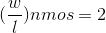
The width of NMOSes are 2*minimum feature size as shown below

Given, minimum feature size is 2*lambda
Therefore, 

and
length l= minimum feature size

Therefore,
----------------------------------------
C)
Add Answer to:
Fig. 3 as follows is an IC layout of a CMOS implementation of a two-input digital...
solve both 2.10 Find the transistor schematic for the CMOS logic circuit realized by the layout...
 solve both
2.10 Find the transistor schematic for the CMOS logic circuit realized by the layout shown in Fig. P2.10. Give the widths of all transistors. AssumeL = 21, where A = 0.4 um. In tabular form, give the area and perimeter of each junction that is not connected to VDD or to ground. VDD Polysilicon 8A n well -p diffusion Active region Out 6/ n diffusion Metal Gnd A Fig. P2.10 D 17.33 The circuit of Fig. P17.33 consists...
solve both
2.10 Find the transistor schematic for the CMOS logic circuit realized by the layout shown in Fig. P2.10. Give the widths of all transistors. AssumeL = 21, where A = 0.4 um. In tabular form, give the area and perimeter of each junction that is not connected to VDD or to ground. VDD Polysilicon 8A n well -p diffusion Active region Out 6/ n diffusion Metal Gnd A Fig. P2.10 D 17.33 The circuit of Fig. P17.33 consists...
Most questions answered within 3 hours.
-
. A 100.0 mL sample of 0.18 M HClO4 is titrated with 0.27 M
LiOH. Determine...
asked 6 minutes ago -
A regression equation that describes the relationship between
the amount of the bill ($) at a...
asked 1 hour ago -
exercise on VSEPR and molecular structrue.
octahedral
SeCl62-
TeCl62-
ClF62-
distorted
SeF62–
IF6–
asked 1 hour ago -
284 mL of a 0.52 M potassium hydroxide solution is added to 467
mL of a...
asked 1 hour ago -
Little’s Law: Val d’Costa is a world famous ski village in the
French Alps. Because of...
asked 2 hours ago -
Find the absolute error D for the calculation if A + B/C=D A=
9.4 +/- 0.4...
asked 2 hours ago -
New Air Heating and Cooling, manufactures furnaces and central
air units. The company pride itself on...
asked 2 hours ago -
A coach uses a new technique to train gymnasts. Seven
gymnasts were randomly selected and their...
asked 4 hours ago -
While rotating the tires on your car you notice a rock [mass =
0.1 Kg] stuck...
asked 6 hours ago -
Using MARS simulator, write MIPS programs according to
the following scenarios: Receive a positive integer number...
asked 8 hours ago -
An object in front of a concave mirror has a real image that is
11.5 cm...
asked 8 hours ago -
Consider the reaction, C3 H8 + O2 --> CO2 + H2O. How many
moles of O2...
asked 10 hours ago