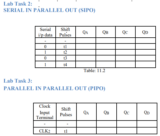
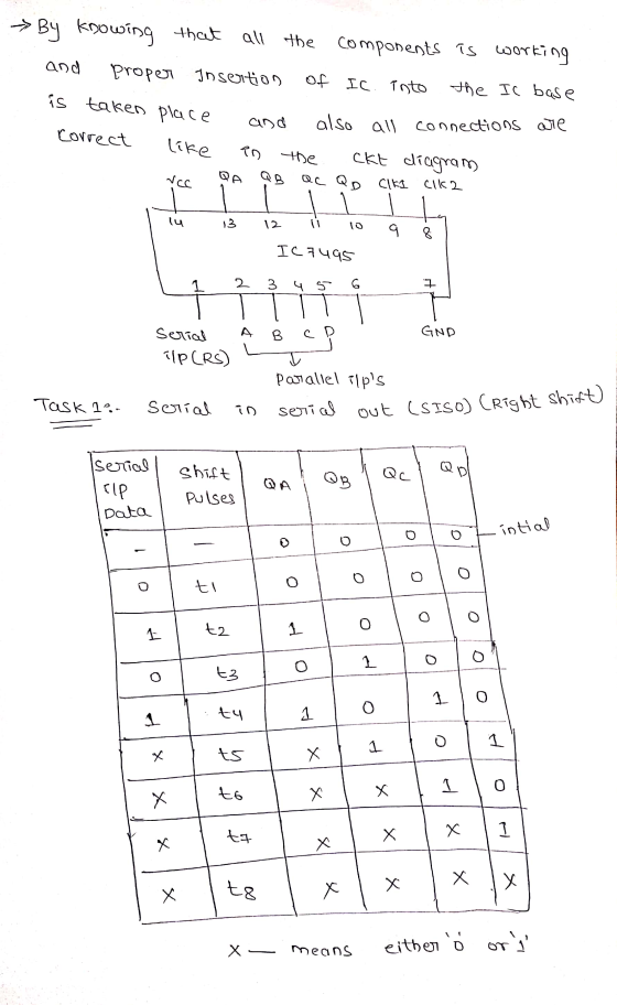
In Lab
1. Check all the components for their working
2. Insert the appropriate IC into the IC base
3. Make connections as shown in the circuit diagram
4. Verify the Truth Table and observe the outputs


Homework Answers

Add Answer to:
In Lab
1. Check all the components for their working
2. Insert the appropriate IC into...
Problem 7. Consider the 74x194 4-bit bidirectional universal shift register shown below Determine the operation of...
 Problem 7. Consider the 74x194 4-bit bidirectional universal shift register shown below Determine the operation of this circuit by filling out the table. Assume that the register is cleared initially as indicated by the first row in the table, and then connected to +5V (before time t), as shown in schematic. Also assume that t 'is that time at which a positive edge occurs in the input signal 'clock'. Si and S0 inputs (given) are used to switch between modes...
1. What is the typical Luminous Intensity of the Vishay TDCR1060M LED Clock Display? (15pt) 2. Th...
1. What is the typical Luminous Intensity of the Vishay TDCR1060M LED Clock Display? (15pt) 2. The Vishay TDCR1060M LED Clock Display emits red light. What is the wavelength of that red light? (15pt) 3. The Vishay TDCR1060M LED Clock Display emits red light. (15pt) What is the frequency of that red light? (Express the answer in THz) 4. The Vishay TDCR1060M LED Clock Display emits red light. (15pt) What is the frequency of that red light? (Express the answer...
Determine the period number of the ufk-4 cos(K+TT/2) discrete time signal! Select one: O A. 34 O ...
 Determine the period number of the ufk-4 cos(K+TT/2) discrete time signal! Select one: O A. 34 O D. Non periodic O E. 34/3 A coil (L 5 mH) is parallel connected to two serially connected resistors (6 kΩ and 4 k2). Calculate the time constant of the above two-pole! Select one: Ο Α.0.5s OC. 5 s Ο D. 0.5 με Ο Ε.0.5 Ms Consider the following sequential network: Z2 Di Ct ㄍ洼 S2 Q2 CLK Choose which function does this...
This is the sequence 1,3,6,10,15 the pattern is addin 1 more than last time but what is the name for this pattern These are called the triangular numbers The sequence is 1 3=1+2 6=1+2+3 10=1+2+3+4 15=1+2+3+4+5 You can also observe this pattern
This is the sequence 1,3,6,10,15 the pattern is addin 1 more than last time but what is the name for this patternThese are called the triangular numbers The sequence is 1 3=1+2 6=1+2+3 10=1+2+3+4 15=1+2+3+4+5 You can also observe this pattern x _________ x xx __________ x xx xxx __________ x xx xxx xxxx to see why they're called triangular numbers. I think the Pythagoreans (around 700 B.C.E.) were the ones who gave them this name. I do know the...
(might be 1 or 2, MCQ questions were having images given with them, which we couldn't...
(might be 1 or 2, MCQ questions were having images given with them, which we couldn't insert, so ignore those questions if you cannot answer, sorry for inconveinience created, i tried to delete them but might be couldn't done all) 3) Single phase induction motors work because: a) The oscillating magnetic field can induce starting torque in a rotor. b) The oscillating magnetic field can induce running torque in a rotor. c) A capacitance or inductance can create the phase...
 Problem 7. Consider the 74x194 4-bit bidirectional universal shift register shown below Determine the operation of this circuit by filling out the table. Assume that the register is cleared initially as indicated by the first row in the table, and then connected to +5V (before time t), as shown in schematic. Also assume that t 'is that time at which a positive edge occurs in the input signal 'clock'. Si and S0 inputs (given) are used to switch between modes...
 Determine the period number of the ufk-4 cos(K+TT/2) discrete time signal! Select one: O A. 34 O D. Non periodic O E. 34/3 A coil (L 5 mH) is parallel connected to two serially connected resistors (6 kΩ and 4 k2). Calculate the time constant of the above two-pole! Select one: Ο Α.0.5s OC. 5 s Ο D. 0.5 με Ο Ε.0.5 Ms Consider the following sequential network: Z2 Di Ct ㄍ洼 S2 Q2 CLK Choose which function does this...
Most questions answered within 3 hours.
-
Calculate the molality, mole-fraction and percent mass of 28.9M
HF at 25 degrees Celcius of the...
asked 6 minutes ago -
A developmental psychologist believes that children raised in
bilingual families will have higher verbal fluency at...
asked 13 minutes ago -
A fast food meal has 5660 kJ of energy. A person uses energy at
a rate...
asked 25 minutes ago -
The pKb for a generic amine(R-NH2)) in
aqueous solution is 6.30. What is its pKa?
asked 27 minutes ago -
The following reactions have the indicated equilibrium constants
at a particular temperature: N2(g) + O2(g) ⇌...
asked 29 minutes ago -
Please Help ASAP.
1Consider the below code which iterates over a linked
list of n nodes...
asked 45 minutes ago -
Determine the air to fuel ratio of:
Canadian natural gas, with 93.9% methane, 4.2% ethane, 0.3%...
asked 45 minutes ago -
A manufacturer of power tools claims that the average amount of
time required to assemble their...
asked 48 minutes ago -
"electron-withdrawing substituents on carbon encourage back
donation", then on the next page he says that "greater...
asked 59 minutes ago -
On December 31, 2016, the shareholders’ equity section of the
balance sheet of R & L...
asked 1 hour ago -
16.7
At t=0s a small "upward" (positive y) pulse centered at x = 5.0
m is...
asked 1 hour ago -
Twitter Users and News: A poll conducted in 2013 found that 52%
of U.S. adult Twitter...
asked 1 hour ago