
Homework Answers

Add Answer to:
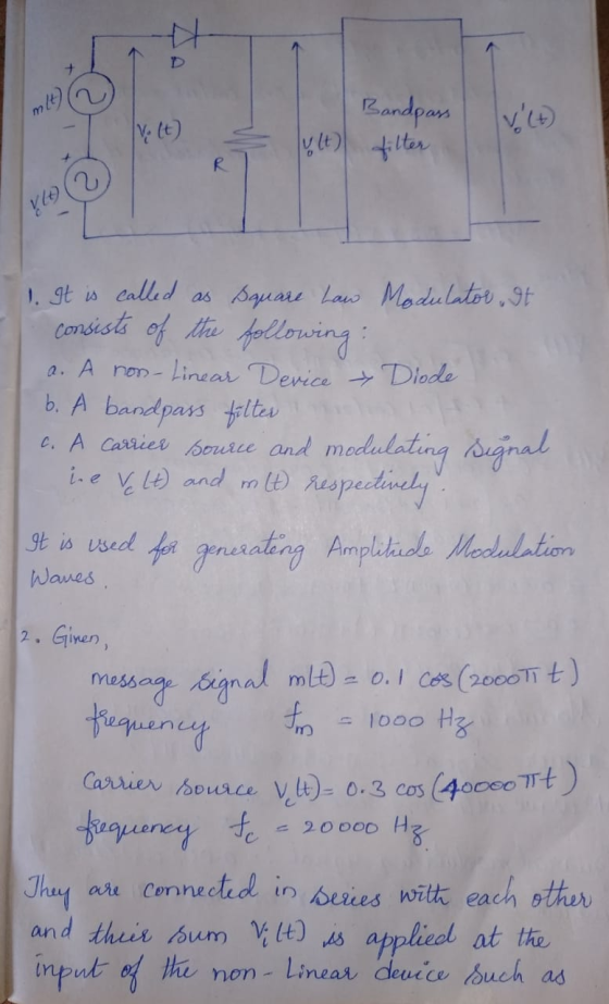
Q: One type of modulators is shown below: y(t) Rs 10 Bandpass filter von Vc(t) 1-...
5) Consider the following second-order bandpass filter. As input voltage, apply V(t) 100Ω, C-4.7 μF. and L-10mH. sin(wt).R in Vout Fig 9: Second-order band-pass filter a) Determine the frequenc...
 5) Consider the following second-order bandpass filter. As input voltage, apply V(t) 100Ω, C-4.7 μF. and L-10mH. sin(wt).R in Vout Fig 9: Second-order band-pass filter a) Determine the frequency response function H(ju) Ve-ju) / Vm(ju) and sketch the magnitude and phase characteristics versus w by calaulation. Calculate the theoretical cutoff frequency of the filter Using PSpice AC analysis, plot magnitude lHju)l and phase ф characteristics of the filter, between 1 Hz-100 KHz b) c)
5) Consider the following second-order bandpass...
5) Consider the following second-order bandpass filter. As input voltage, apply V(t) 100Ω, C-4.7 μF. and L-10mH. sin(wt).R in Vout Fig 9: Second-order band-pass filter a) Determine the frequency response function H(ju) Ve-ju) / Vm(ju) and sketch the magnitude and phase characteristics versus w by calaulation. Calculate the theoretical cutoff frequency of the filter Using PSpice AC analysis, plot magnitude lHju)l and phase ф characteristics of the filter, between 1 Hz-100 KHz b) c)
5) Consider the following second-order bandpass...
Consider the series RLC bandpass filter shown in (Figure 1). The filter has a quality of...
 Consider the series RLC bandpass filter shown in (Figure 1). The filter has a quality of 2 and a center frequency of 8 kHz. The input to the filter is vi (t) = 23 cos wt V. Suppose that C = 5 nF. Figure < 1 of 1 + VLC с L HE + + Vi R} R V. Part E Find the voltage drop across the series combination of the inductor and capacitor when w=10w, Suppose that vlc (t)...
1. The system shown is used for scrambling audio signals. The output signal, y(t) is the...
 1. The system shown is used for scrambling audio signals. The output signal, y(t) is the scrambled version of the input m(t). Find the spectrum of the scrambled signal y(t): Y(f) Mf) m(t) vt) Low-pass filter 0-15 kHz - (Scrambled output) - 15 kHz | 15 kHz f kHz 2 cos 30,000 t
choose one of the multiple choice answers above. please show all work Question: 10 CIRCUIT Y...
 choose one of the multiple choice answers above.
please show all work
Question: 10 CIRCUIT Y FIG.10 (5 Marks) Statement: Consider the RC-coupled amplifier circuit illustrated in Fig. 10 (CIRCUIT Y). Sketching relevant output (Vc-Ic) characteristics, decide Q-point coordinates and DC load-line details (of the NPN-BJT/Si circuit of Fig. 10 of Circuit Y). Further, establish an appropriate AC-load line and decide the maximum swing of the output voltage across Rload with respect to the Q-point. Assume the input signal at...
choose one of the multiple choice answers above.
please show all work
Question: 10 CIRCUIT Y FIG.10 (5 Marks) Statement: Consider the RC-coupled amplifier circuit illustrated in Fig. 10 (CIRCUIT Y). Sketching relevant output (Vc-Ic) characteristics, decide Q-point coordinates and DC load-line details (of the NPN-BJT/Si circuit of Fig. 10 of Circuit Y). Further, establish an appropriate AC-load line and decide the maximum swing of the output voltage across Rload with respect to the Q-point. Assume the input signal at...
please pick one of the multiple choice options above. show all work, thank you Question 9...
 please pick one of the multiple choice options above.
show all work, thank you
Question 9 CIRCUIT X/FIG.9 (5 Marks) Statement: Consider the RC-coupled amplifier circuit illustrated in Fig. 9 (CIRCUIT X). Sketching relevant output (Vc-Ic) characteristics that decide Q-point coordinates and DC load-line details (of the NPN-BJT/Si circuit of Fig. 9 of Circuit X) Further, establish an appropriate AC-load line and decide the maximum swing of the output voltage across Rload with respect to the Q-point. Assume the input...
please pick one of the multiple choice options above.
show all work, thank you
Question 9 CIRCUIT X/FIG.9 (5 Marks) Statement: Consider the RC-coupled amplifier circuit illustrated in Fig. 9 (CIRCUIT X). Sketching relevant output (Vc-Ic) characteristics that decide Q-point coordinates and DC load-line details (of the NPN-BJT/Si circuit of Fig. 9 of Circuit X) Further, establish an appropriate AC-load line and decide the maximum swing of the output voltage across Rload with respect to the Q-point. Assume the input...
 5) Consider the following second-order bandpass filter. As input voltage, apply V(t) 100Ω, C-4.7 μF. and L-10mH. sin(wt).R in Vout Fig 9: Second-order band-pass filter a) Determine the frequency response function H(ju) Ve-ju) / Vm(ju) and sketch the magnitude and phase characteristics versus w by calaulation. Calculate the theoretical cutoff frequency of the filter Using PSpice AC analysis, plot magnitude lHju)l and phase ф characteristics of the filter, between 1 Hz-100 KHz b) c)
5) Consider the following second-order bandpass...
5) Consider the following second-order bandpass filter. As input voltage, apply V(t) 100Ω, C-4.7 μF. and L-10mH. sin(wt).R in Vout Fig 9: Second-order band-pass filter a) Determine the frequency response function H(ju) Ve-ju) / Vm(ju) and sketch the magnitude and phase characteristics versus w by calaulation. Calculate the theoretical cutoff frequency of the filter Using PSpice AC analysis, plot magnitude lHju)l and phase ф characteristics of the filter, between 1 Hz-100 KHz b) c)
5) Consider the following second-order bandpass...
 Consider the series RLC bandpass filter shown in (Figure 1). The filter has a quality of 2 and a center frequency of 8 kHz. The input to the filter is vi (t) = 23 cos wt V. Suppose that C = 5 nF. Figure < 1 of 1 + VLC с L HE + + Vi R} R V. Part E Find the voltage drop across the series combination of the inductor and capacitor when w=10w, Suppose that vlc (t)...
 1. The system shown is used for scrambling audio signals. The output signal, y(t) is the scrambled version of the input m(t). Find the spectrum of the scrambled signal y(t): Y(f) Mf) m(t) vt) Low-pass filter 0-15 kHz - (Scrambled output) - 15 kHz | 15 kHz f kHz 2 cos 30,000 t
 choose one of the multiple choice answers above.
please show all work
Question: 10 CIRCUIT Y FIG.10 (5 Marks) Statement: Consider the RC-coupled amplifier circuit illustrated in Fig. 10 (CIRCUIT Y). Sketching relevant output (Vc-Ic) characteristics, decide Q-point coordinates and DC load-line details (of the NPN-BJT/Si circuit of Fig. 10 of Circuit Y). Further, establish an appropriate AC-load line and decide the maximum swing of the output voltage across Rload with respect to the Q-point. Assume the input signal at...
choose one of the multiple choice answers above.
please show all work
Question: 10 CIRCUIT Y FIG.10 (5 Marks) Statement: Consider the RC-coupled amplifier circuit illustrated in Fig. 10 (CIRCUIT Y). Sketching relevant output (Vc-Ic) characteristics, decide Q-point coordinates and DC load-line details (of the NPN-BJT/Si circuit of Fig. 10 of Circuit Y). Further, establish an appropriate AC-load line and decide the maximum swing of the output voltage across Rload with respect to the Q-point. Assume the input signal at...
 please pick one of the multiple choice options above.
show all work, thank you
Question 9 CIRCUIT X/FIG.9 (5 Marks) Statement: Consider the RC-coupled amplifier circuit illustrated in Fig. 9 (CIRCUIT X). Sketching relevant output (Vc-Ic) characteristics that decide Q-point coordinates and DC load-line details (of the NPN-BJT/Si circuit of Fig. 9 of Circuit X) Further, establish an appropriate AC-load line and decide the maximum swing of the output voltage across Rload with respect to the Q-point. Assume the input...
please pick one of the multiple choice options above.
show all work, thank you
Question 9 CIRCUIT X/FIG.9 (5 Marks) Statement: Consider the RC-coupled amplifier circuit illustrated in Fig. 9 (CIRCUIT X). Sketching relevant output (Vc-Ic) characteristics that decide Q-point coordinates and DC load-line details (of the NPN-BJT/Si circuit of Fig. 9 of Circuit X) Further, establish an appropriate AC-load line and decide the maximum swing of the output voltage across Rload with respect to the Q-point. Assume the input...
Most questions answered within 3 hours.
-
A diver springs upward with an initial speed of 2.1 m/s from a
3.5-m board.
(a)...
asked 5 minutes ago -
Using α = 0.05, test if the mean weight change
is less than 0 if a...
asked 9 minutes ago -
In an isobaric compression process, the volume of steam is
reduced from 1 Mpa and 773...
asked 9 minutes ago -
blood glucose level for obese patient population have
a mean of 100 with a standard deviation...
asked 10 minutes ago -
Which of the following mutations is MOST likely to be
recessive?
A.
Deletion of a haplo-insufficient...
asked 14 minutes ago -
The U.S. Department of Transportation, National Highway Traffic
Safety Administration, reported that 77% of all fatally...
asked 26 minutes ago -
For 1 through 11, create an expression using the relational
operators, the logical operators, and variable...
asked 39 minutes ago -
Remove all recursion from the following grammar:
S -> Aa | Bb
A -> Aa |...
asked 32 minutes ago -
The production budget for Manner Company shows units to be
produced as follows: July, 550; August,...
asked 42 minutes ago -
Your group is required to develop a comprehensive Business plan
that will be used as a...
asked 46 minutes ago -
a radio station transmits at 78.1 mhz. a hz is an inverse
second. how far apart...
asked 1 hour ago -
Write the equilibrium expression for the dissociation in
water for CH5N, C2H5O2COOH, H3AsO4, KClO2, HC2H2ClO2.
asked 1 hour ago