
Homework Answers


Add Answer to:
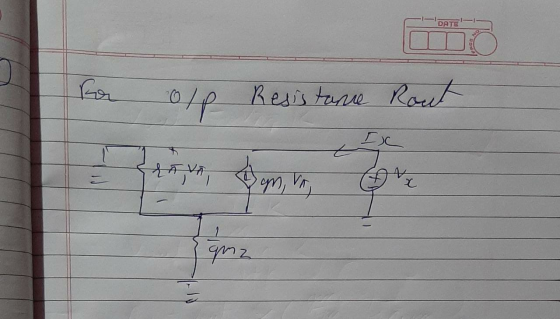
Q2: In the following BUT circuit, small signal parameters for Q1 and Q2 are labeled symbolically...
Please show step on how to solve this. Problem 4 Assume the current through M1 and Q1, M2 and Q1 is lmA.Voc.bias (1). Please calculate the small-signal resistance r and r2 (2). Please calculate the s...
 Please show step on how to solve this.
Problem 4 Assume the current through M1 and Q1, M2 and Q1 is lmA.Voc.bias (1). Please calculate the small-signal resistance r and r2 (2). Please calculate the small-signal gain in both case (a) and VDC,bias M Vout r Vout Vin Vin MI (NMOS) M2 (PMOS) Q1 (NPN) ls = 1 × 10-18[A]. β 100, va = 100[V],
Problem 4 Assume the current through M1 and Q1, M2 and Q1 is lmA.Voc.bias (1)....
Please show step on how to solve this.
Problem 4 Assume the current through M1 and Q1, M2 and Q1 is lmA.Voc.bias (1). Please calculate the small-signal resistance r and r2 (2). Please calculate the small-signal gain in both case (a) and VDC,bias M Vout r Vout Vin Vin MI (NMOS) M2 (PMOS) Q1 (NPN) ls = 1 × 10-18[A]. β 100, va = 100[V],
Problem 4 Assume the current through M1 and Q1, M2 and Q1 is lmA.Voc.bias (1)....
2. For the common-emitter amplifier. B= 50. Vcc=12 a) Draw small signal circuit b) Find vout/vin...
 2. For the common-emitter amplifier. B= 50. Vcc=12 a) Draw small signal circuit b) Find vout/vin Find Zin and Zou Vcc R1 27k R2 2.2k Zout Zin Vo 4 C1 16 BIG Q1 NPN V1 C2 V R3 15k RE 1.2k BIG
Problem 4 +5 volts a) Find Ic1, Ic2, and Ic3. You may neglect all b) Find the resistance looking into the base of 10 m c) Find the small signal voltage gain Vout/Vin d) What is the approximate DC val...
 Problem 4 +5 volts a) Find Ic1, Ic2, and Ic3. You may neglect all b) Find the resistance looking into the base of 10 m c) Find the small signal voltage gain Vout/Vin d) What is the approximate DC value of Vx? base currents. transistor Q1. (Hint: use the results of (b)!) Q1 +Vin C=infinite 200 for all transistors Beta 50 ohms Vout Q2 Q3 5 volts
Problem 4 +5 volts a) Find Ic1, Ic2, and Ic3. You may neglect...
Problem 4 +5 volts a) Find Ic1, Ic2, and Ic3. You may neglect all b) Find the resistance looking into the base of 10 m c) Find the small signal voltage gain Vout/Vin d) What is the approximate DC value of Vx? base currents. transistor Q1. (Hint: use the results of (b)!) Q1 +Vin C=infinite 200 for all transistors Beta 50 ohms Vout Q2 Q3 5 volts
Problem 4 +5 volts a) Find Ic1, Ic2, and Ic3. You may neglect...
3. Consider the following circuit. Q1 is identical to Q2 and p- 100. Q3 is identical...
 3. Consider the following circuit. Q1 is identical to Q2 and p- 100. Q3 is identical to Q4 and B Assume VBE.on-0.7V, VT-25mV. oofor Q1 and Q3, and r, 400 k2 for Q3 and Q4. Vid Vil -Va for differential mode operation, Vicm Vil vi2 for common mode operation, Vo Vo2-Vol for differentially taken output (a) Design Ra to have the bias current lcs 2 mA. (b) Find the differential mode voltage gain for differentially taken output (As Vo/ Via)...
Problem 2: Consider the following amplifier circuit. All capacitors are infinite valued. Voc RB1 Rc1 Rc2...
 Problem 2: Consider the following amplifier circuit. All capacitors are infinite valued. Voc RB1 Rc1 Rc2 0 Q1 Vout RB2 Rout1 Q2 Rout2 Rint R1 Rin2 Rsig + IEI Vsig Voc SINE() IE2 a. Specify the type of amplifier in each stage. b. Draw the small signal model of this amplifier and include the early effect. c. Derive an expression for Rout1 and Rout2 including early effect. d. Derive expressions for Rin1 and Rin2. Ignore the early effect. e. Derive...
 Please show step on how to solve this.
Problem 4 Assume the current through M1 and Q1, M2 and Q1 is lmA.Voc.bias (1). Please calculate the small-signal resistance r and r2 (2). Please calculate the small-signal gain in both case (a) and VDC,bias M Vout r Vout Vin Vin MI (NMOS) M2 (PMOS) Q1 (NPN) ls = 1 × 10-18[A]. β 100, va = 100[V],
Problem 4 Assume the current through M1 and Q1, M2 and Q1 is lmA.Voc.bias (1)....
Please show step on how to solve this.
Problem 4 Assume the current through M1 and Q1, M2 and Q1 is lmA.Voc.bias (1). Please calculate the small-signal resistance r and r2 (2). Please calculate the small-signal gain in both case (a) and VDC,bias M Vout r Vout Vin Vin MI (NMOS) M2 (PMOS) Q1 (NPN) ls = 1 × 10-18[A]. β 100, va = 100[V],
Problem 4 Assume the current through M1 and Q1, M2 and Q1 is lmA.Voc.bias (1)....
 2. For the common-emitter amplifier. B= 50. Vcc=12 a) Draw small signal circuit b) Find vout/vin Find Zin and Zou Vcc R1 27k R2 2.2k Zout Zin Vo 4 C1 16 BIG Q1 NPN V1 C2 V R3 15k RE 1.2k BIG
 Problem 4 +5 volts a) Find Ic1, Ic2, and Ic3. You may neglect all b) Find the resistance looking into the base of 10 m c) Find the small signal voltage gain Vout/Vin d) What is the approximate DC value of Vx? base currents. transistor Q1. (Hint: use the results of (b)!) Q1 +Vin C=infinite 200 for all transistors Beta 50 ohms Vout Q2 Q3 5 volts
Problem 4 +5 volts a) Find Ic1, Ic2, and Ic3. You may neglect...
Problem 4 +5 volts a) Find Ic1, Ic2, and Ic3. You may neglect all b) Find the resistance looking into the base of 10 m c) Find the small signal voltage gain Vout/Vin d) What is the approximate DC value of Vx? base currents. transistor Q1. (Hint: use the results of (b)!) Q1 +Vin C=infinite 200 for all transistors Beta 50 ohms Vout Q2 Q3 5 volts
Problem 4 +5 volts a) Find Ic1, Ic2, and Ic3. You may neglect...
 3. Consider the following circuit. Q1 is identical to Q2 and p- 100. Q3 is identical to Q4 and B Assume VBE.on-0.7V, VT-25mV. oofor Q1 and Q3, and r, 400 k2 for Q3 and Q4. Vid Vil -Va for differential mode operation, Vicm Vil vi2 for common mode operation, Vo Vo2-Vol for differentially taken output (a) Design Ra to have the bias current lcs 2 mA. (b) Find the differential mode voltage gain for differentially taken output (As Vo/ Via)...
 Problem 2: Consider the following amplifier circuit. All capacitors are infinite valued. Voc RB1 Rc1 Rc2 0 Q1 Vout RB2 Rout1 Q2 Rout2 Rint R1 Rin2 Rsig + IEI Vsig Voc SINE() IE2 a. Specify the type of amplifier in each stage. b. Draw the small signal model of this amplifier and include the early effect. c. Derive an expression for Rout1 and Rout2 including early effect. d. Derive expressions for Rin1 and Rin2. Ignore the early effect. e. Derive...
Most questions answered within 3 hours.
-
Calculate the number density of argon gas at a temperature of
24C and a pressure of...
asked 1 hour ago -
Alternative
Classification
How to Estimate
Probabilities from Data? ( For continuous Attributes)
And How to generate...
asked 1 hour ago -
An explosion breaks a 20.0-kg object into three parts. The
object is initially moving at a...
asked 2 hours ago -
Calculate the approximate number of residues of Rubisco, which
is involved in carbon fixation in plants,...
asked 3 hours ago -
Other decisions about scientific claims can have a much broader
impact.ENERGYarrow-10x10.png, environment, health, security - all...
asked 4 hours ago -
I need to write a research paper and work cited about this
topic: The United States...
asked 4 hours ago -
Hello! I was wondering if I could have some help?
If the vapor pressure of carvone...
asked 4 hours ago -
An economist wants to estimate the mean per capita income (in
thousands of dollars) for a...
asked 5 hours ago -
What would be the input/output characteristic of a circuit
obtained by putting two of your 2's-complementers...
asked 5 hours ago -
In Drosophila, the transition from the syncytial blastoderm
stage to the cellular blastoderm stage is a...
asked 5 hours ago -
Project management question:
Name 3 different types of resources (hint: humans are one
type)
asked 5 hours ago -
Consider the following reaction: C 2H 2( g) + 2H 2( g) C 2H 6(
g)...
asked 6 hours ago