Draw a complete step-by-step CMOS process flow with a p-type substrate for n well formation including...
Draw a complete step-by-step CMOS process flow with a p-type substrate for n well formation including a layout mask for each lithography step, showing an NMOSFET, a PMOSFET, and an undoped polysilicon resistor. The size of both MOS transistors is W=25 micro-meters, L=0.25micro- m, and the length of the source/drain regions are Ls=0.5 micrometers. The resistor value is R=35k.and the strip width for resistors is set at 0.5micro meters.
Homework Answers
Step 1) Start with a P-substrate.
Step 2 ) Oxidation -- Grow SiO2 on top of Silicon wafer at -900
to -1200C with H2O or O2 in oxidation furnace, So that layer of
SiO2 will be formed on top of P-substrate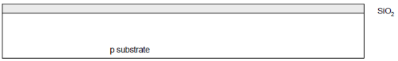
Step 3) Photoresist -- Photoresist is light sensitive organic
polymer that will soften when exposed to light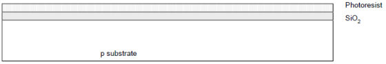
Step 4) Lithography -- For lithography, expose the photoresist
so that it will soften and then strip off the part to form
n-well
Step 5) Etch -- The wafer is exposed to hydrofluoric acid (HF), to etch the SiO2 part

Step 6) Strip Photoresist -- Strip the remaining photoresist

Step 7) Diffusion and Ion implantation to form n-well
n-well is formed with diffusion and ion implantation. Diffusion is a process in which the wafer is placed in furnace and exposed to Arsenic gas. When heat is applied to the furnace, the Arsanic (As) gas atoms will diffuse into the exposed Si wafer to form n-well. These As atoms are blocked by SiO2 layer.

Step 8) Strip Oxide -- Strip off the remaining SiO2 using
HF
Step 9 ) Polysilicon -- Deposit a thin layer of gate oxide then
on top of gate oxide, polysilicon is deposited by process of CVD
(Chemical Vapor Deposition).
Step 10) Polysilicon Patterning -- Same lithography process is
followed to form required pattern
Add Answer to:
Draw a complete step-by-step CMOS process flow with a p-type
substrate for n well formation including...
Most questions answered within 3 hours.
-
Suppose that XX is a random variable with mean 16 and standard
deviation 5 . Also...
asked 36 minutes ago -
Calculate the number density of argon gas at a temperature of
24C and a pressure of...
asked 3 hours ago -
Alternative
Classification
How to Estimate
Probabilities from Data? ( For continuous Attributes)
And How to generate...
asked 3 hours ago -
An explosion breaks a 20.0-kg object into three parts. The
object is initially moving at a...
asked 4 hours ago -
Calculate the approximate number of residues of Rubisco, which
is involved in carbon fixation in plants,...
asked 5 hours ago -
Other decisions about scientific claims can have a much broader
impact.ENERGYarrow-10x10.png, environment, health, security - all...
asked 6 hours ago -
I need to write a research paper and work cited about this
topic: The United States...
asked 6 hours ago -
Hello! I was wondering if I could have some help?
If the vapor pressure of carvone...
asked 7 hours ago -
An economist wants to estimate the mean per capita income (in
thousands of dollars) for a...
asked 7 hours ago -
What would be the input/output characteristic of a circuit
obtained by putting two of your 2's-complementers...
asked 7 hours ago -
In Drosophila, the transition from the syncytial blastoderm
stage to the cellular blastoderm stage is a...
asked 8 hours ago -
Project management question:
Name 3 different types of resources (hint: humans are one
type)
asked 8 hours ago