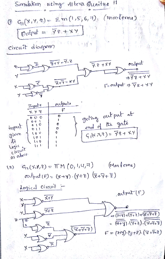
Design a logic circuit (NOR-NOR gates only) , simulate and test the circuit using an Altera Quartus II Software based on the Boolean function below: G1(X, Y, Z) = ∑ m (1,5,6,7) G2 (X, Y, Z) = ∏ M (0,1...
Design a logic circuit (NOR-NOR gates only) , simulate and test the circuit using an Altera Quartus II Software based on the Boolean function below:
G1(X, Y, Z) = ∑ m (1,5,6,7)
G2 (X, Y, Z) = ∏ M (0,1,4,7)
I'm not sure how to design the circuit and how to verify the output using Altera Quartus II, anyone help? Thanks :)
Homework Answers


Add Answer to:
Design a logic circuit (NOR-NOR gates only) , simulate and test the circuit using an Altera Quartus II Software based on the Boolean function below: G1(X, Y, Z) = ∑ m (1,5,6,7) G2 (X, Y, Z) = ∏ M (0,1...
Implement this Boolean Expression on a breadboard using NOR gates Part A: Z =XY+X 'Y' Implement...
 Implement this Boolean Expression on a breadboard using NOR
gates
Part A: Z =XY+X 'Y' Implement this Boolean expression using only NOR gates. Apply De Morgan's law and Boolean laws for the expression to represent it only using NOR operation. Your implementation should use the minimum number of gates (4 NOR gates) required
Implement this Boolean Expression on a breadboard using NOR
gates
Part A: Z =XY+X 'Y' Implement this Boolean expression using only NOR gates. Apply De Morgan's law and Boolean laws for the expression to represent it only using NOR operation. Your implementation should use the minimum number of gates (4 NOR gates) required
Design a combinational circuit with three inputs, x , y, and z, and three outputs, A,...
Design a combinational circuit with three inputs, x , y, and z, and three outputs, A, B , and C . When the binary input is 0, 1, 2, or 3, the binary output is one greater than the input. When the binary input is 4, 5, 6, or 7, the binary output is two less than the input. 1) Truth table 2) Logic circuit 3) Boolean function of A using minterms ( use Boolean algebra) 4) Boolean function of...
Implement the Boolean function F(w,x,y,z) = Σm(3, 4, 5, 1 1, 12, 13, 14, 15) using a minimum number of NAND gates only.
Implement the Boolean function F(w,x,y,z) = Σm(3, 4, 5, 1 1, 12, 13, 14, 15) using a minimum number of NAND gates only. Write the minimal logic expression (no need to draw the circuit).
We are interested in designing a circuit that implements the following three Boolean functions: 3. h(x,y,z)=Σm(1,4,6)...
 We are interested in designing a circuit that implements the following three Boolean functions: 3. h(x,y,z)=Σm(1,4,6) f1x,y,z)- > m(1,4,6) y-m35) (x,y, z) Σ m (2,4,6,7) 左 You are supposed to implement the circuit with a decoder constructed with NAND gates (a) [12pt] Start by drawing the block diagram of a NAND-based decoder with three inputs (x,y,z), labelling all the outputs with their corresponding Boolean functions (b) [8pt) Using a new block diagram of the NAND-based decoder, implement the circuit using...
Tim Question 1 Atte 20 pts 2H 24 Design a 1-bit Full Adder using NOR gates...
 Tim Question 1 Atte 20 pts 2H 24 Design a 1-bit Full Adder using NOR gates only, you must include and show: Truth tables, detail logic gate circuit designs, and Boolean expressions Upload Choose a File 20 pts Question 2 Design a 4-bit Full Adder with inputs (Xo...X3, Yo...Y3) in which inputs X are connect to two 4-bit registers via four 2-to-1 Multiplexers and inputs Y are connected to two other 4-bit registers via four 2-to-1 Multiplexers. In this case...
1. (15 pts) Simplify the following Boolean functions using K-maps: a. F(x,y,z) = (1,4,5,6,7) b. F(x,...
 1. (15 pts) Simplify the following Boolean functions using K-maps: a. F(x,y,z) = (1,4,5,6,7) b. F(x, y, z) = (xy + xyz + xyz c. F(A,B,C,D) = 20,2,4,5,6,7,8,10,13,15) d. F(A,B,C,D) = A'B'C'D' + AB'C + B'CD' + ABCD' + BC'D e. F(A,B,C,D,E) = (0,1,4,5,16,17,21,25,29) 2. (12 pts) Consider the combinational logic circuit below and answer the following: a. Derive the Boolean expressions for Fi and F2 as functions of A, B, C, and D. b. List the complete truth table...
Design a PLA that implements the followingthree boolean function A(w,x,y,z) = ?m(4, 5, 7, 12, 13,...
Design a PLA that implements the followingthree boolean function A(w,x,y,z) = ?m(4, 5, 7, 12, 13, 15) B(w,x,y,z) = ?m(0, 1, 4, 5, 8, 9, 11, 12, 13, 15) C(w,x,y,z) = ?m(0, 1, 2, 3, 6, 7, 8, 9, 10, 11, 14) a) Use Karnaugh Maps to optimal each function and its complement. b)Select the three optimal functions to use in the PLA. C)Optimize the equation(s) using Karnaugh Map(s). d.Draw the circuit (Don't forget the clock).
a. Design and implement a combinational circuit with four inputs w,x, y and z and four outputs A, B,C and D using CMOS...
 a. Design and implement a combinational circuit with four inputs w,x, y and z and four outputs A, B,C and D using CMOS transistors. When the binary input is 0, 1, 2,3, 4, 5, 6 or 7 the binary output is three greater than the input. When the binary input is 8,10,11,12,13,14 or 15 the binary output is five less than the input. b. Draw the mask layout with Ln Lp 0.6 um, Wn- 4.8 um and Wp- 9.6 um...
Design and implement a combinational circuit with four inputs w,x, y and z and four outputs A, B ,C and D using CMOS transistors. When the binary input is 0, 1, 2,3,4,5,6 or 7 the binary output is fi...
Design and implement a combinational circuit with four inputs w,x, y and z and four outputs A, B ,C and D using CMOS transistors. When the binary input is 0, 1, 2,3,4,5,6 or 7 the binary output is five greater than the input. When the binary input is 8,,10,11,12,13,14 or 15 the binary output is seven less than the input. for question (a) find the troth table for the inputs (ABCD) then implement using K-map to find the equations to...
 Implement this Boolean Expression on a breadboard using NOR
gates
Part A: Z =XY+X 'Y' Implement this Boolean expression using only NOR gates. Apply De Morgan's law and Boolean laws for the expression to represent it only using NOR operation. Your implementation should use the minimum number of gates (4 NOR gates) required
Implement this Boolean Expression on a breadboard using NOR
gates
Part A: Z =XY+X 'Y' Implement this Boolean expression using only NOR gates. Apply De Morgan's law and Boolean laws for the expression to represent it only using NOR operation. Your implementation should use the minimum number of gates (4 NOR gates) required
 We are interested in designing a circuit that implements the following three Boolean functions: 3. h(x,y,z)=Σm(1,4,6) f1x,y,z)- > m(1,4,6) y-m35) (x,y, z) Σ m (2,4,6,7) 左 You are supposed to implement the circuit with a decoder constructed with NAND gates (a) [12pt] Start by drawing the block diagram of a NAND-based decoder with three inputs (x,y,z), labelling all the outputs with their corresponding Boolean functions (b) [8pt) Using a new block diagram of the NAND-based decoder, implement the circuit using...
 Tim Question 1 Atte 20 pts 2H 24 Design a 1-bit Full Adder using NOR gates only, you must include and show: Truth tables, detail logic gate circuit designs, and Boolean expressions Upload Choose a File 20 pts Question 2 Design a 4-bit Full Adder with inputs (Xo...X3, Yo...Y3) in which inputs X are connect to two 4-bit registers via four 2-to-1 Multiplexers and inputs Y are connected to two other 4-bit registers via four 2-to-1 Multiplexers. In this case...
 1. (15 pts) Simplify the following Boolean functions using K-maps: a. F(x,y,z) = (1,4,5,6,7) b. F(x, y, z) = (xy + xyz + xyz c. F(A,B,C,D) = 20,2,4,5,6,7,8,10,13,15) d. F(A,B,C,D) = A'B'C'D' + AB'C + B'CD' + ABCD' + BC'D e. F(A,B,C,D,E) = (0,1,4,5,16,17,21,25,29) 2. (12 pts) Consider the combinational logic circuit below and answer the following: a. Derive the Boolean expressions for Fi and F2 as functions of A, B, C, and D. b. List the complete truth table...
 a. Design and implement a combinational circuit with four inputs w,x, y and z and four outputs A, B,C and D using CMOS transistors. When the binary input is 0, 1, 2,3, 4, 5, 6 or 7 the binary output is three greater than the input. When the binary input is 8,10,11,12,13,14 or 15 the binary output is five less than the input. b. Draw the mask layout with Ln Lp 0.6 um, Wn- 4.8 um and Wp- 9.6 um...
 a. Design and implement a combinational circuit with four inputs w,x, y and z and four outputs A, B,C and D using CMOS transistors. When the binary input is 0, 1, 2,3, 4, 5, 6 or 7 the binary output is three greater than the input. When the binary input is 8,10,11,12,13,14 or 15 the binary output is five less than the input. b. Draw the mask layout with Ln Lp 0.6 um, Wn- 4.8 um and Wp- 9.6 um...
Most questions answered within 3 hours.
-
The cash account for American Medical Co. at April 30 indicated
a balance of $10,785. The...
asked 1 minute ago -
aluminum maker Alcoa has a beta of about 1.86, whereas Hormel
Foods has a beta of...
asked 2 minutes ago -
Hewtex Electronics manufactures two products, headsets and
electronic calculators, and sells them nationally to wholesalers
and...
asked 4 minutes ago -
Describe how to measure benefits, including specific examples of
clinical and financial benefits that can be...
asked 17 minutes ago -
Costs associated with the manufacture of miniature
high-sensitivity piezoresistive pressure transducers is $74,000 per
year. A...
asked 32 minutes ago -
Given the following information for Jane Cole complete schedule
D of 1040 through part III and...
asked 31 minutes ago -
Why doesn't a small piece of uranium go naturally into a chain
reaction?
A) A small...
asked 36 minutes ago -
Last year’s freshman class at Big State University totaled 5,324
students. Of those, 1,254 received a...
asked 44 minutes ago -
The transverse displacement of a stretched string from
equilibrium as a function of time and position...
asked 48 minutes ago -
Do a detailed SWOT analysis for a small Agribusiness company in
Brazil
asked 48 minutes ago -
Which two measures of excellence are often in
conflict/contradiction with each other (and therefore difficult to...
asked 47 minutes ago -
Which of the following factors does not
negatively impact operating cash flows?
Group of answer choices...
asked 49 minutes ago