
Homework Answers
Answer #1

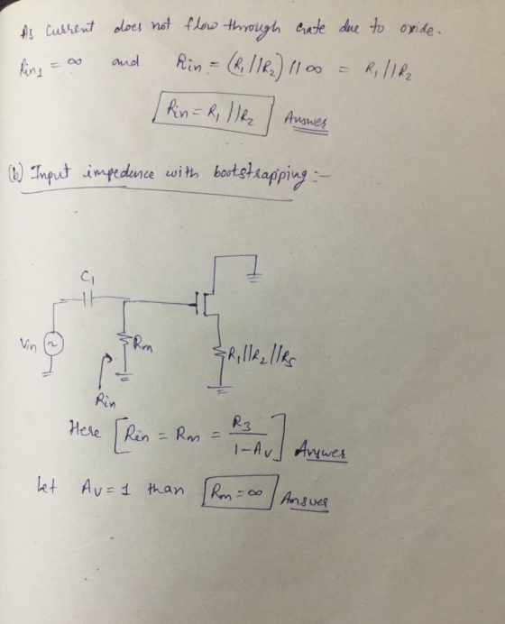
aualynis capacit Rth op R2 i Capacito i replaced aih cht circuit and 'oo Xine R2 is between 11p nade G, and df nade D,」R au be rph a by Rn and Rn ty esivg milles themem ivid wittaut bootdiup bieing tv)
Ani Answes nee with boots Ci Vin) 3
Know the answer?
Add Answer to:
3. The circuit from Fig.3 is a source follower with bootstrapping. The reason for bootstrapping is related to the resistive divider R1 and R2 for generating the gate bias voltage of M1 02 UT Fig....
Not the answer you're looking for?
Ask your own homework help question.
Our experts will answer your question WITHIN MINUTES for Free.
Similar Homework Help Questions
Lab ll: Voltage Follower ECE 210: 1. For the following circuit, Theoretically calculate the peak ...
 URGENT!! PLEASE HELP! be clear and answer all questions
clearly!!
Lab ll: Voltage Follower ECE 210: 1. For the following circuit, Theoretically calculate the peak voltage across R3 (Vo) an ved R1-2.2k0 2.17362(Actual) R2 = 3.3kN-3.Z44KAL (Actual) R3-10kΩ 9.873M. (Actual) Vin- 1kHz Triangle wave, 2V peak, NO DC offset e) R Draw the output waveform Vo: UI R1 R2 X-Axis 0.1 msec/div 2. Remove the resistor R2 to create the following circuit Draw the output waveform Vo: U1 R1 R3...
URGENT!! PLEASE HELP! be clear and answer all questions
clearly!!
Lab ll: Voltage Follower ECE 210: 1. For the following circuit, Theoretically calculate the peak voltage across R3 (Vo) an ved R1-2.2k0 2.17362(Actual) R2 = 3.3kN-3.Z44KAL (Actual) R3-10kΩ 9.873M. (Actual) Vin- 1kHz Triangle wave, 2V peak, NO DC offset e) R Draw the output waveform Vo: UI R1 R2 X-Axis 0.1 msec/div 2. Remove the resistor R2 to create the following circuit Draw the output waveform Vo: U1 R1 R3...
ADVERTISEMENT
Need Online Homework Help?
Ask
a QuestionGet Answers For Free
Most questions answered within 3 hours.
Most questions answered within 3 hours.
ADVERTISEMENT
ADVERTISEMENT
Active Questions
-
A bicyclist starting at rest produces a constant angular
acceleration of 1.10 rad/s2 for wheels that...
asked 7 minutes ago -
The
half-life of a radioactive source is 14.0 minutes. How much time
must elapse before the...
asked 5 minutes ago -
Given P(Ec ) = 0.43, P(F) = 0.52, and P(EF) = 0.18.
Find P( E |...
asked 52 minutes ago -
Consider two empty containers A and B whose volumes are
10mL and 20mL respectively. 1mL of...
asked 55 minutes ago -
QUESTION 6
Determine the linear momentum of a 2,800 kg houseboat going 3
m/s.
9,100 kg.m/s...
asked 1 hour ago -
Jor-el throws a ball upward from the top of a 728 foot building
on the planet...
asked 1 hour ago -
Which of the following will most likely to happen if Federal
Reserve Bank decreases the money...
asked 56 minutes ago -
You’ve just joined the investment banking firm of Dewey,
Cheatum, and Howe. They’ve offered you two...
asked 50 minutes ago -
An air conditioner cools 226 m^3/min of humid air at 36 oC and
98% relative humidity...
asked 49 minutes ago -
Vaughn Manufacturing acquires a coal mine at a cost of $1870000.
Intangible development costs total $354000....
asked 59 minutes ago -
Question 5
What effect would a decrease in
temperature have on pressure, assuming that volume
(T)...
asked 1 hour ago -
Draw the Lewis dot structures for the following molecules. None
of the atoms have a formal...
asked 1 hour ago
ADVERTISEMENT