
Homework Answers
F1 (x, y, z) =  m (0, 1,
2)
m (0, 1,
2)
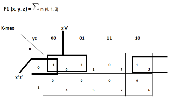
The Simplified SOP of F1 = x'y'+x'z'
F2 (x, y, z) =  M (2, 3,
6, 7)
M (2, 3,
6, 7)
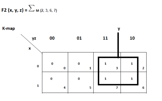
The Simplified SOP of F2 = y
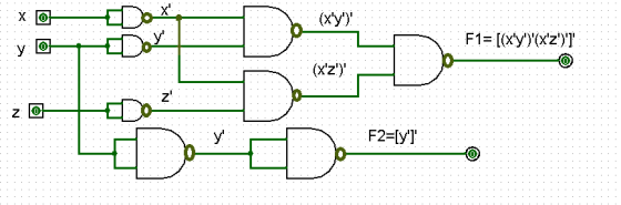
Single Logic Circuit for F1 & F2 Using AND, OR & NOT gates

Circuit Using NAND gates
F1 = x'y'+x'z'
[F1']' = [(x'y'+x'z')']'.
F1 = [(x'y')'(x'z')']'
F2 = y
[F2']' = [y']'
Add Answer to:
5. Express the functions F1 and F2 shown in the truth table below in sum-of- products...
Design a circuit with three inputs (A, B, C) and two outputs (F1, F2). The first...
 Design a circuit with three inputs (A, B, C) and two outputs (F1, F2). The first output F1 is logic 1 if the number of l’s in the binary number is less than the number of O's, otherwise F1 is logic 0. The second output F2 is 1 if the binary input is 2, 4, 5, 6,7 otherwise the second output F2 is logic 0. a. Derive the truth-table for F1 and F2 as a function of the 3 inputs....
Design a circuit with three inputs (A, B, C) and two outputs (F1, F2). The first...
 Design a circuit with three inputs (A, B, C) and two outputs (F1, F2). The first output F1 is 1 when the binary input is 2, 3, 4, 7, otherwise the first output F1 is logic 0. The second output F2 is 1 when the input variables have more l's than 0's. The output is 0 otherwise. Input/ Output ABC F1 F2 000 001 010 011 100 101 a. Derive the truth-table for F1 and F2 as a function of...
(1)Try to use NAND gates to achieve the truth table function of an XOR gate (2)...
(1)Try to use NAND gates to achieve the truth table function of an XOR gate (2) Try to design a clicker for three people, it just needs two people to agree to pass. A,B,C indicate the people, 0 means don't agree, 1 means agree. If it passes the result is 1. Please write the truth table, the SOP (sum of products) equation and draw the logic circuit for it. (3)Use a Karnaugh-map to simplify the following Boolean function: F= AB'C'+A'B'C'+AB'C+A'B'C+AB...
Assume you have the following truth tables for function F1(w,x,y,z). Express F1 in sum-of-products form, in...
 Assume you have the following truth tables for function
F1(w,x,y,z).
Express F1 in sum-of-products form, in other words, determine
the equation.
w'x'y'z+w'x'yz+wx'y'z+wx'y'z'+wxy'z'+wxy'z+wxyz'+wxyz
Simplify each function of the previous problem using Karnaugh
map????
"1 0 1 0 1 0 0 0 0 0 1 0 1 1 1 1 1 20101010101010101 y 0 0 1 1 0 0 1 1 0 0 1 1 0 0 1 1 X0000-11100001111 w00000000-1111111
Assume you have the following truth tables for function
F1(w,x,y,z).
Express F1 in sum-of-products form, in other words, determine
the equation.
w'x'y'z+w'x'yz+wx'y'z+wx'y'z'+wxy'z'+wxy'z+wxyz'+wxyz
Simplify each function of the previous problem using Karnaugh
map????
"1 0 1 0 1 0 0 0 0 0 1 0 1 1 1 1 1 20101010101010101 y 0 0 1 1 0 0 1 1 0 0 1 1 0 0 1 1 X0000-11100001111 w00000000-1111111
Truth tables of three logic functions F1, F2 and F3 given above. Implement the function F1, F2 and F3 using 3 to 8 decoder
 Q2A: Truth tables of three logic functions F1, F2 and F3 given above. Implement the function F1, F2 and F3 using 3 to 8 decoder? (Assume a 3to8 decoder component given to you, if required you may use minimum number of additional logic gates to support your design with 3 to 8 decoder) (Points) Q2B: Write HDL code to implement the above function F1, F2 and F3. All three function should include in on HDL code. In you HDL code use...
1. Find the Boolean expression of the truth table. Then simplify it and convert it into...
 1. Find the Boolean expression of the truth table. Then simplify it and convert it into the least amount of logic gates possible. AB Output 100 011 101 2. Find the POS form of the Boolean expressions below. Find the truth table and logic minimization method of it. Show its gate level implementation, and show the same gate level implementation using only NAND gates. A(X,Y,Z)= m(0,2,4,6) B(X,Y,2)={m(0,4,5) 3. Create a J-k Flip Flop using a D-Flip Flop. Show its truth...
Having the next Boolean functions: F1(x,y,z)-П (1, 3, 5) . F2(x,y,z)-Σ (0, 2, 4, 5) . 1. Make one...
 Computer architecture
Having the next Boolean functions: F1(x,y,z)-П (1, 3, 5) . F2(x,y,z)-Σ (0, 2, 4, 5) . 1. Make one logic gate design circuit, using AND, OR and NOT logic gates (20 points). 2. Design two 4-to-1 selectors, one for each Boolean function (20 points) 3. Design one 3-to-8 decoder to solve both Boolean functions (20 points) 4. Design a 8x2 ROM to solve both Boolean functions (20 points) 5. Design a 3x5x2 PLA to solve both Boolean functions...
Computer architecture
Having the next Boolean functions: F1(x,y,z)-П (1, 3, 5) . F2(x,y,z)-Σ (0, 2, 4, 5) . 1. Make one logic gate design circuit, using AND, OR and NOT logic gates (20 points). 2. Design two 4-to-1 selectors, one for each Boolean function (20 points) 3. Design one 3-to-8 decoder to solve both Boolean functions (20 points) 4. Design a 8x2 ROM to solve both Boolean functions (20 points) 5. Design a 3x5x2 PLA to solve both Boolean functions...
Given the Function F1(w, x, y, z) and F2(x0, x1, y0, y1), write the truth table...
 Given the Function F1(w, x, y, z) and F2(x0, x1, y0, y1), write
the truth table for each function. F1(w, x, y, z) - Specified by
the lab instructor F2(x0, x1, y0, y1) is a two bit adder. The
function F2(x0, x1, y0, y1) has 3 outputs - 2 bits for the sum and
1 bit for the carry out Cout
3. Given the Function F1(w, x, y, z) and F2(x0, X1, yo, yı), write the truth table for each...
Given the Function F1(w, x, y, z) and F2(x0, x1, y0, y1), write
the truth table for each function. F1(w, x, y, z) - Specified by
the lab instructor F2(x0, x1, y0, y1) is a two bit adder. The
function F2(x0, x1, y0, y1) has 3 outputs - 2 bits for the sum and
1 bit for the carry out Cout
3. Given the Function F1(w, x, y, z) and F2(x0, X1, yo, yı), write the truth table for each...
X 1. Determine the truth table for the above circuit. A B C 0 0 0...
 X 1. Determine the truth table for the above circuit. A B C 0 0 0 0 0 0 1 0 0 1 1 1 0 0 1 0 1 1 1 0 111 2. Determine the Karnaugh Map for the above circuit and do both an SOP minimization (the left KAI) and a POS minimization (the right KM). Write the minimized Boolean expressions below the corresponding Karnaugh Map BC ВС 00 01 11 10 00 01 11 10 0...
Create a truth table to implement AND logic using only NAND gates. Draw the circuit diagram...
Create a truth table to implement AND logic using only NAND gates. Draw the circuit diagram (schematic) for the implementation. Do the same for OR logic using only NOR gates.
 Design a circuit with three inputs (A, B, C) and two outputs (F1, F2). The first output F1 is logic 1 if the number of l’s in the binary number is less than the number of O's, otherwise F1 is logic 0. The second output F2 is 1 if the binary input is 2, 4, 5, 6,7 otherwise the second output F2 is logic 0. a. Derive the truth-table for F1 and F2 as a function of the 3 inputs....
 Design a circuit with three inputs (A, B, C) and two outputs (F1, F2). The first output F1 is 1 when the binary input is 2, 3, 4, 7, otherwise the first output F1 is logic 0. The second output F2 is 1 when the input variables have more l's than 0's. The output is 0 otherwise. Input/ Output ABC F1 F2 000 001 010 011 100 101 a. Derive the truth-table for F1 and F2 as a function of...
 Assume you have the following truth tables for function
F1(w,x,y,z).
Express F1 in sum-of-products form, in other words, determine
the equation.
w'x'y'z+w'x'yz+wx'y'z+wx'y'z'+wxy'z'+wxy'z+wxyz'+wxyz
Simplify each function of the previous problem using Karnaugh
map????
"1 0 1 0 1 0 0 0 0 0 1 0 1 1 1 1 1 20101010101010101 y 0 0 1 1 0 0 1 1 0 0 1 1 0 0 1 1 X0000-11100001111 w00000000-1111111
Assume you have the following truth tables for function
F1(w,x,y,z).
Express F1 in sum-of-products form, in other words, determine
the equation.
w'x'y'z+w'x'yz+wx'y'z+wx'y'z'+wxy'z'+wxy'z+wxyz'+wxyz
Simplify each function of the previous problem using Karnaugh
map????
"1 0 1 0 1 0 0 0 0 0 1 0 1 1 1 1 1 20101010101010101 y 0 0 1 1 0 0 1 1 0 0 1 1 0 0 1 1 X0000-11100001111 w00000000-1111111
 Q2A: Truth tables of three logic functions F1, F2 and F3 given above. Implement the function F1, F2 and F3 using 3 to 8 decoder? (Assume a 3to8 decoder component given to you, if required you may use minimum number of additional logic gates to support your design with 3 to 8 decoder) (Points) Q2B: Write HDL code to implement the above function F1, F2 and F3. All three function should include in on HDL code. In you HDL code use...
 1. Find the Boolean expression of the truth table. Then simplify it and convert it into the least amount of logic gates possible. AB Output 100 011 101 2. Find the POS form of the Boolean expressions below. Find the truth table and logic minimization method of it. Show its gate level implementation, and show the same gate level implementation using only NAND gates. A(X,Y,Z)= m(0,2,4,6) B(X,Y,2)={m(0,4,5) 3. Create a J-k Flip Flop using a D-Flip Flop. Show its truth...
 Computer architecture
Having the next Boolean functions: F1(x,y,z)-П (1, 3, 5) . F2(x,y,z)-Σ (0, 2, 4, 5) . 1. Make one logic gate design circuit, using AND, OR and NOT logic gates (20 points). 2. Design two 4-to-1 selectors, one for each Boolean function (20 points) 3. Design one 3-to-8 decoder to solve both Boolean functions (20 points) 4. Design a 8x2 ROM to solve both Boolean functions (20 points) 5. Design a 3x5x2 PLA to solve both Boolean functions...
Computer architecture
Having the next Boolean functions: F1(x,y,z)-П (1, 3, 5) . F2(x,y,z)-Σ (0, 2, 4, 5) . 1. Make one logic gate design circuit, using AND, OR and NOT logic gates (20 points). 2. Design two 4-to-1 selectors, one for each Boolean function (20 points) 3. Design one 3-to-8 decoder to solve both Boolean functions (20 points) 4. Design a 8x2 ROM to solve both Boolean functions (20 points) 5. Design a 3x5x2 PLA to solve both Boolean functions...
 Given the Function F1(w, x, y, z) and F2(x0, x1, y0, y1), write
the truth table for each function. F1(w, x, y, z) - Specified by
the lab instructor F2(x0, x1, y0, y1) is a two bit adder. The
function F2(x0, x1, y0, y1) has 3 outputs - 2 bits for the sum and
1 bit for the carry out Cout
3. Given the Function F1(w, x, y, z) and F2(x0, X1, yo, yı), write the truth table for each...
Given the Function F1(w, x, y, z) and F2(x0, x1, y0, y1), write
the truth table for each function. F1(w, x, y, z) - Specified by
the lab instructor F2(x0, x1, y0, y1) is a two bit adder. The
function F2(x0, x1, y0, y1) has 3 outputs - 2 bits for the sum and
1 bit for the carry out Cout
3. Given the Function F1(w, x, y, z) and F2(x0, X1, yo, yı), write the truth table for each...
 X 1. Determine the truth table for the above circuit. A B C 0 0 0 0 0 0 1 0 0 1 1 1 0 0 1 0 1 1 1 0 111 2. Determine the Karnaugh Map for the above circuit and do both an SOP minimization (the left KAI) and a POS minimization (the right KM). Write the minimized Boolean expressions below the corresponding Karnaugh Map BC ВС 00 01 11 10 00 01 11 10 0...
Most questions answered within 3 hours.
-
In 2005, Derrek Lee led the National Baseball League with a
0.335 batting average, meaning that...
asked 37 seconds ago -
In order for corporations to behave ethically, they must,
ultimately, give up the profit motive.
...
asked 38 seconds ago -
Blue Spruce Corp. owns equipment that cost $63,400 when
purchased on January 1, 2017. It has...
asked 20 minutes ago -
A lottery exists where balls numbered 1 to 17 are placed in an
urn. To win,...
asked 1 hour ago -
Please explain steps:
An 80 kg swimmer steps off a platform 10 m above the water...
asked 1 hour ago -
26) Briefly describe, using words or simple diagrams, the
chemiosmotic theory for coupling oxidation to phosphorylation...
asked 3 hours ago -
Suppose that XX is a random variable with mean 16 and standard
deviation 5 . Also...
asked 4 hours ago -
Calculate the number density of argon gas at a temperature of
24C and a pressure of...
asked 7 hours ago -
Alternative
Classification
How to Estimate
Probabilities from Data? ( For continuous Attributes)
And How to generate...
asked 7 hours ago -
An explosion breaks a 20.0-kg object into three parts. The
object is initially moving at a...
asked 8 hours ago -
Calculate the approximate number of residues of Rubisco, which
is involved in carbon fixation in plants,...
asked 9 hours ago -
Other decisions about scientific claims can have a much broader
impact.ENERGYarrow-10x10.png, environment, health, security - all...
asked 10 hours ago