

Homework Answers

Add Answer to:
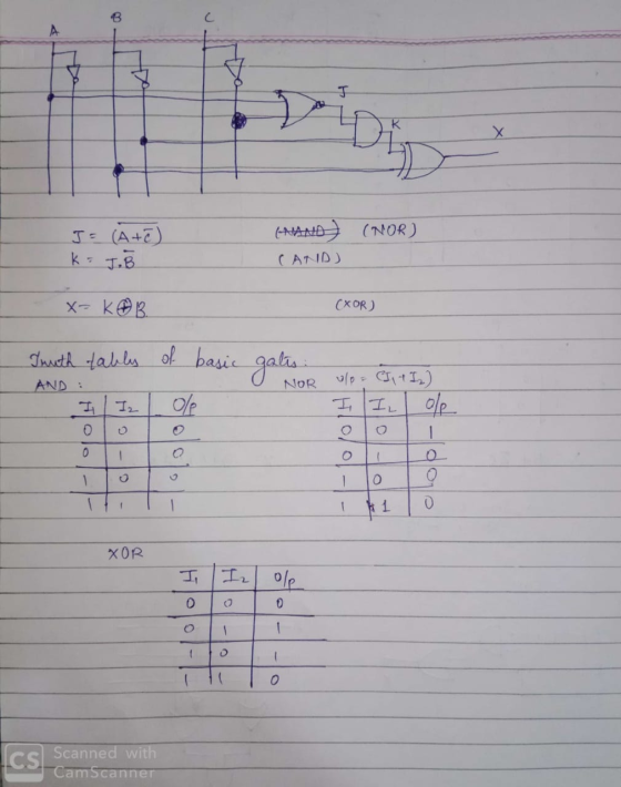
X 1. Determine the truth table for the above circuit. A B C 0 0 0...
3. For the following circuit: B a. Give the truth table for F. b. Complete the...
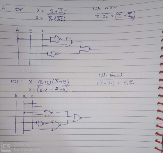
 3. For the following circuit: B a. Give the truth table for F. b. Complete the following K-map and use it to give the minimized POS form for F(A,B,C). CIAB 00 01 11 10 C. Use boolean axioms and theorems on POS expression obtained in (b) to get the SOP form. The final SOP expression should have a maximum of two terms. d. Draw the logic circuit for the SOP form.
Create a truth table to implement AND logic using only NAND gates. Draw the circuit diagram...
Create a truth table to implement AND logic using only NAND gates. Draw the circuit diagram (schematic) for the implementation. Do the same for OR logic using only NOR gates.
(1)Try to use NAND gates to achieve the truth table function of an XOR gate (2)...
(1)Try to use NAND gates to achieve the truth table function of an XOR gate (2) Try to design a clicker for three people, it just needs two people to agree to pass. A,B,C indicate the people, 0 means don't agree, 1 means agree. If it passes the result is 1. Please write the truth table, the SOP (sum of products) equation and draw the logic circuit for it. (3)Use a Karnaugh-map to simplify the following Boolean function: F= AB'C'+A'B'C'+AB'C+A'B'C+AB...
(18 pts) Given the Boolean function F(A, B, C, D) = Σ (0, 1, 2, 3,...
 (18 pts) Given the Boolean function F(A, B, C, D) = Σ (0, 1, 2, 3, 4, 5, 7, 8, 10, 12, 14) a. Draw a Karnaugh Map. b. Identify the prime implicants of F. c. Identify all Essential Prime Implicants of F. d. Derive minimal SOP expressions for F e. Derive minimal POS expressions for F. f. Assume each inverter has a cost of 1, each 2-input NAND gate has a cost of 2, and 4-input NAND gate has...
Build a digital circuit that can add two binary numbers of two bit each and shows...
 Build a digital circuit that can add two binary numbers of two
bit each and shows the answer using three LEDs
1. Find the canonical equations of the following characteristics
table in SOP and POS
2. Convert them and implement the SOP canonical equation
only.
3. Simplify each equation SOP and POS and implement each one
using logic gates.
4. Convert each circuit into its respective NAND-NAND and
NOR_NOR and implement them using logic gates.
Objetivo: Construir un circuito digital...
Build a digital circuit that can add two binary numbers of two
bit each and shows the answer using three LEDs
1. Find the canonical equations of the following characteristics
table in SOP and POS
2. Convert them and implement the SOP canonical equation
only.
3. Simplify each equation SOP and POS and implement each one
using logic gates.
4. Convert each circuit into its respective NAND-NAND and
NOR_NOR and implement them using logic gates.
Objetivo: Construir un circuito digital...
A combination circuit is specified by the following Boolean functions listed below. h(a, b, c) = b,c' + a'c Implement the circuit with a 3x8 decoder. Provide truth table and drawing the l...
 A combination circuit is specified by the following Boolean functions listed below. h(a, b, c) = b,c' + a'c Implement the circuit with a 3x8 decoder. Provide truth table and drawing the logic/circuit diagram. Use the block diagram for the decoder provided in Figure A4 in supplements. Please label the inputs and outputs clearly. Note: use single 3x8 decoder Question 2 (15 points] A priority encoder is an encoder circuit that includes the Truth Table of a priority function. The...
Question 2 1. Formulate the minimized SOP and POS Boolean expression for the following truth table...
 Question 2 1. Formulate the minimized SOP and POS Boolean expression for the following truth table using Karnaugh map techniques. Out of the SOP and POS implementations, which is cheaper in terms of number of transistors? You can assume two transistors per input for a gate. (10 points) A B C Output 0 0 0 1 1 0 0 1 0 1 0 0 0 1 0 1 1
Consider the following function. (8 <A ri eve n of products) expression. Don't draw the gate...
 Consider the following function. (8 <A ri eve n of products) expression. Don't draw the gate 1131 0 diagram yet. (b) Use De Morgan's Laws or "bubble pushing" to convert the SOP expression to something that can be directly implemented with only NAND/NOR/inverter gates. (c) Now draw the schematic (logic gates) for the resulting NAND/NOR/inverter circuit.
I need help with this Logic circuit problem. Problem #2 Given the logic function F(a,b,c) cabctab'c'+a'c'c'tabb'...
 I need help with this Logic circuit problem.
Problem #2 Given the logic function F(a,b,c) cabctab'c'+a'c'c'tabb' a) Normalize the product terms and write the function again. Answer: F(a,b,c) b) Find a minimal SOP expression using a Karnaugh Map Answer: F(a,b,c) c) Based on the result of the previous part find an expression that minimizes the discrete gate count using gates of any kinod. Answer: Fla,b,c)- d) Find a minimal POS expression using a Karnaugh Map Answer: F(a,b,c)
I need help with this Logic circuit problem.
Problem #2 Given the logic function F(a,b,c) cabctab'c'+a'c'c'tabb' a) Normalize the product terms and write the function again. Answer: F(a,b,c) b) Find a minimal SOP expression using a Karnaugh Map Answer: F(a,b,c) c) Based on the result of the previous part find an expression that minimizes the discrete gate count using gates of any kinod. Answer: Fla,b,c)- d) Find a minimal POS expression using a Karnaugh Map Answer: F(a,b,c)
Given the following Karnaugh map AB CD 00 01 11 10 01 011 Draw a circuit...
 Given the following Karnaugh map AB CD 00 01 11 10 01 011 Draw a circuit that realizes the function above using one 8-to-1 multiplexer and any number of NAND gates. Observe that A, B and C are connected to the select inputs, SO, S1, and S2. 4-to-1 MUX -10 12 13 14 15 16 17 So Si S2 ABC
 3. For the following circuit: B a. Give the truth table for F. b. Complete the following K-map and use it to give the minimized POS form for F(A,B,C). CIAB 00 01 11 10 C. Use boolean axioms and theorems on POS expression obtained in (b) to get the SOP form. The final SOP expression should have a maximum of two terms. d. Draw the logic circuit for the SOP form.
 (18 pts) Given the Boolean function F(A, B, C, D) = Σ (0, 1, 2, 3, 4, 5, 7, 8, 10, 12, 14) a. Draw a Karnaugh Map. b. Identify the prime implicants of F. c. Identify all Essential Prime Implicants of F. d. Derive minimal SOP expressions for F e. Derive minimal POS expressions for F. f. Assume each inverter has a cost of 1, each 2-input NAND gate has a cost of 2, and 4-input NAND gate has...
 Build a digital circuit that can add two binary numbers of two
bit each and shows the answer using three LEDs
1. Find the canonical equations of the following characteristics
table in SOP and POS
2. Convert them and implement the SOP canonical equation
only.
3. Simplify each equation SOP and POS and implement each one
using logic gates.
4. Convert each circuit into its respective NAND-NAND and
NOR_NOR and implement them using logic gates.
Objetivo: Construir un circuito digital...
Build a digital circuit that can add two binary numbers of two
bit each and shows the answer using three LEDs
1. Find the canonical equations of the following characteristics
table in SOP and POS
2. Convert them and implement the SOP canonical equation
only.
3. Simplify each equation SOP and POS and implement each one
using logic gates.
4. Convert each circuit into its respective NAND-NAND and
NOR_NOR and implement them using logic gates.
Objetivo: Construir un circuito digital...
 A combination circuit is specified by the following Boolean functions listed below. h(a, b, c) = b,c' + a'c Implement the circuit with a 3x8 decoder. Provide truth table and drawing the logic/circuit diagram. Use the block diagram for the decoder provided in Figure A4 in supplements. Please label the inputs and outputs clearly. Note: use single 3x8 decoder Question 2 (15 points] A priority encoder is an encoder circuit that includes the Truth Table of a priority function. The...
 Question 2 1. Formulate the minimized SOP and POS Boolean expression for the following truth table using Karnaugh map techniques. Out of the SOP and POS implementations, which is cheaper in terms of number of transistors? You can assume two transistors per input for a gate. (10 points) A B C Output 0 0 0 1 1 0 0 1 0 1 0 0 0 1 0 1 1
 Consider the following function. (8 <A ri eve n of products) expression. Don't draw the gate 1131 0 diagram yet. (b) Use De Morgan's Laws or "bubble pushing" to convert the SOP expression to something that can be directly implemented with only NAND/NOR/inverter gates. (c) Now draw the schematic (logic gates) for the resulting NAND/NOR/inverter circuit.
 I need help with this Logic circuit problem.
Problem #2 Given the logic function F(a,b,c) cabctab'c'+a'c'c'tabb' a) Normalize the product terms and write the function again. Answer: F(a,b,c) b) Find a minimal SOP expression using a Karnaugh Map Answer: F(a,b,c) c) Based on the result of the previous part find an expression that minimizes the discrete gate count using gates of any kinod. Answer: Fla,b,c)- d) Find a minimal POS expression using a Karnaugh Map Answer: F(a,b,c)
I need help with this Logic circuit problem.
Problem #2 Given the logic function F(a,b,c) cabctab'c'+a'c'c'tabb' a) Normalize the product terms and write the function again. Answer: F(a,b,c) b) Find a minimal SOP expression using a Karnaugh Map Answer: F(a,b,c) c) Based on the result of the previous part find an expression that minimizes the discrete gate count using gates of any kinod. Answer: Fla,b,c)- d) Find a minimal POS expression using a Karnaugh Map Answer: F(a,b,c)
 Given the following Karnaugh map AB CD 00 01 11 10 01 011 Draw a circuit that realizes the function above using one 8-to-1 multiplexer and any number of NAND gates. Observe that A, B and C are connected to the select inputs, SO, S1, and S2. 4-to-1 MUX -10 12 13 14 15 16 17 So Si S2 ABC
Most questions answered within 3 hours.
-
Using MARS simulator, write MIPS programs according to
the following scenarios: Receive a positive integer number...
asked 42 minutes ago -
An object in front of a concave mirror has a real image that is
11.5 cm...
asked 55 minutes ago -
Consider the reaction, C3 H8 + O2 --> CO2 + H2O. How many
moles of O2...
asked 2 hours ago -
You and your opponent both roll a fair die. If you both roll the
same number,...
asked 2 hours ago -
In a study of the accuracy of fast food drive-through orders,
Restaurant A had 257 accurate...
asked 2 hours ago -
Identify and describe in detail the four categories of
institutions that could be included in a...
asked 3 hours ago -
In python
class Customer:
def __init__(self, customer_id, last_name, first_name, phone_number, address):
self._customer_id = int(customer_id)
self._last_name =...
asked 3 hours ago -
What is an example of a limitation in implementing a new
ERP system and how it...
asked 3 hours ago -
In a section of 9.7cm of an artery with a radius of 2.6mm there
is a...
asked 3 hours ago -
the two carboxylic acid groups of aspartic acid have different
acidities with pKa values of 2.1...
asked 3 hours ago -
Would CuCO3 aqueous salt combined with calcium chloride
form a solid precipitate? If so, what would...
asked 3 hours ago -
How do ECM Solutions assist in embedding a culture of continuous
improvement in an organization? (Project...
asked 3 hours ago