
a) Is this a n-channel or p-channel? why?
b) Does this appear to be a long channel or a short channel device? Why?
c) Based on the above IV curve you want to estimate Vt, explain your approach to obtain it.
d) The high frequency limit of operation of a JFET is dependent on the dimension and physical properties of the device. Describe three different approaches to improve the high frequency response in a JFET
Homework Answers
a) n-channel
A N-Channel JFET is a JFET whose channel is composed of primarily electrons as the charge carrier. This means that when the transistor is turned on, it is primarily the movement of electrons which constitutes the current flow.


b) Beyond VDS = VP, there is a short pinch-off channel
of length, ℓpo.As VDS increases, most of additional
voltage simply
drops across ℓpo as this region is depleted of
carriers and hence highly resistive. The voltage drop across
channel length, Lch remain as VP. Beyond pinch-off
then ID = VP/RAP (VDS>VP).

What happens when negative voltage, says VGS = -2V, is applied to gate with respect to source (with VDS=0).The p+n junction are now reverse biased from the start, the channel is narrower,and channel resistance is now larger than in the VGS =0 case.

c)

It is observed that as the negative gate bias voltage is increased
(1) The maximum saturation drain current becomes smaller because the conducting channel now becomes narrower.
(2) Pinch-off voltage is reached at a lower value of drain current ID than when VGS = 0. When an external bias of, say – 1 V is applied between the gate and the source, the gate-channel junctions are reverse-biased even when drain current, ID is zero. Hence the depletion regions are already penetrating the channel to a certain extent when drain-| source voltage, VDS is zero. Due to this reason, a smaller voltage drop along the channel (i.e. smaller than that for VGS = 0) will increase the depletion regions to the point where 1 they pinch-off the current. Consequently, the pinch-off voltage VP is reached at a lower 1 drain current, ID when VGS = 0.
(3) The ohmic region portion decreases.
(4) Value of drain-source voltage VDS for the avalanche breakdown of the gate junction is reduced.
Value of drain-source voltage, VDS for breakdown with the increase in negative bias voltage is reduced simply due to the fact that gate-source voltage, VGS keeps adding to the I reverse bias at the junction produced by current flow. Thus the maximum value of VDS I that can be applied to a FET is the lowest voltage which causes avalanche breakdown. It is also observed that with VGS = 0, ID saturates at IDSS and the characteristic shows VP = 4 V. When an external bias of – 1 V is applied, the gate-channel junctions still require -4 V to achieve pinch-off. It means that a 3 V drop is now required along the channel instead of the previous 4.0 V. Obviously, this drop of 3 V can be achieved with a lower value of drain current, Similarly when VGS = – 2 V and – 3 V, pinch-off is achieved with 2 V and 1 V respectively, along the channel. These drops of 2 V and 1 V are, of course, achieved with further reduced values of drain current, ID. It is further observed that when the gate-source bias is numerically equal to pinch-off voltage, VP (-4 V in this case), no channel drop is required and, therefore, drain current, ID is zero. The gate-source bias voltage required to reduce drain current, ID to zero is designated the gate-source cut-off voltage, VGS /0FF) and, as explained,
Hence for working of JFET in the pinch-off or active region it is necessary that the following conditions be fulfilled.
VP < VDS < VDS (max)
VGS (OFF)< VGS < 0
0 < ID < IDSS
Hence for working of JFET in the pinch-off or active region, it is necessary that the following conditions be fulfilled.
VP < VDS < VDS (max)
VGS (OFF)< VGS < 0
0 < ID < IDSS
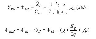
The threshold voltage equals the sum of the flatband voltage, twice the bulk potential and the voltage across the oxide due to the depletion layer charge,
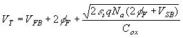
where the flat band voltage, VFB, is given by:
Add Answer to:
a) Is this a n-channel or p-channel? why?
b) Does this appear to be a long...
A common source amplifier circuit based on a single n-channel MOSFET is shown in Figure 4b. Assume that the transconductance gm-60 mS (equivalent to mA/ V) and drain source resistance, os,...
 A common source amplifier circuit based on a single n-channel MOSFET is shown in Figure 4b. Assume that the transconductance gm-60 mS (equivalent to mA/ V) and drain source resistance, os, is so large it may be neglected. 0) Calculate the open circuit voltage gain Av Yout/ Vis. i) The amplifier has a load of 10 k2. Determine the current gain Va. = 12 V 150k 4k3 Vout Vin 200k GND = 0 V Figure 4b a) State the name...
10. Write a one-page summary of the attached paper? INTRODUCTION Many problems can develop in activated...
10. Write a one-page summary of the attached paper? INTRODUCTION Many problems can develop in activated sludge operation that adversely affect effluent quality with origins in the engineering, hydraulic and microbiological components of the process. The real "heart" of the activated sludge system is the development and maintenance of a mixed microbial culture (activated sludge) that treats wastewater and which can be managed. One definition of a wastewater treatment plant operator is a "bug farmer", one who controls the aeration...
I need Summary of this Paper i dont need long summary i need What methodology they used , what is the purpose of this p...
 I need Summary of this Paper i dont need long summary i need
What methodology they used , what is the purpose of this paper and
some conclusions and contributes of this paper. I need this for my
Finishing Project so i need this ASAP please ( IN 1-2-3 HOURS
PLEASE !!!)
Budgetary Policy and Economic Growth Errol D'Souza The share of capital expenditures in government expenditures has been slipping and the tax reforms have not yet improved the income...
I need Summary of this Paper i dont need long summary i need
What methodology they used , what is the purpose of this paper and
some conclusions and contributes of this paper. I need this for my
Finishing Project so i need this ASAP please ( IN 1-2-3 HOURS
PLEASE !!!)
Budgetary Policy and Economic Growth Errol D'Souza The share of capital expenditures in government expenditures has been slipping and the tax reforms have not yet improved the income...
Discussion questions 1. What is the link between internal marketing and service quality in the ai...
 Discussion questions
1. What is the link between internal marketing and service
quality in the airline industry?
2. What internal marketing programmes could British Airways
put into place to avoid further internal unrest? What potential is
there to extend auch programmes to external partners?
3. What challenges may BA face in implementing an internal
marketing programme to deliver value to its customers?
(1981)ǐn the context ofbank marketing ths theme has bon pururd by other, nashri oriented towards the identification of...
Discussion questions
1. What is the link between internal marketing and service
quality in the airline industry?
2. What internal marketing programmes could British Airways
put into place to avoid further internal unrest? What potential is
there to extend auch programmes to external partners?
3. What challenges may BA face in implementing an internal
marketing programme to deliver value to its customers?
(1981)ǐn the context ofbank marketing ths theme has bon pururd by other, nashri oriented towards the identification of...
I need Summary of this Paper i dont need long summary i need What methodology they used , what is the purpose of this...
 I need Summary of this Paper i dont need long summary i need
What methodology they used , what is the purpose of this paper and
some conclusions and contributes of this paper. I need this for my
Finishing Project so i need this ASAP please ( IN 1-2-3 HOURS
PLEASE !!!)
SPECIAL ARTICLES tole of Monetary Policy C Rangarajan What should be the objectives of monetary policy? Does the objective of price stability conflict with the goal of achieving...
I need Summary of this Paper i dont need long summary i need
What methodology they used , what is the purpose of this paper and
some conclusions and contributes of this paper. I need this for my
Finishing Project so i need this ASAP please ( IN 1-2-3 HOURS
PLEASE !!!)
SPECIAL ARTICLES tole of Monetary Policy C Rangarajan What should be the objectives of monetary policy? Does the objective of price stability conflict with the goal of achieving...
SYNOPSIS The product manager for coffee development at Kraft Canada must decide whether to introduce the...
 SYNOPSIS The product manager for coffee development at Kraft Canada must decide whether to introduce the company's new line of single-serve coffee pods or to await results from the product's launch in the United States. Key strategic decisions include choosing the target market to focus on and determining the value proposition to emphasize. Important questions are also raised in regard to how the new product should be branded, the flavors to offer, whether Kraft should use traditional distribution channels or...
 A common source amplifier circuit based on a single n-channel MOSFET is shown in Figure 4b. Assume that the transconductance gm-60 mS (equivalent to mA/ V) and drain source resistance, os, is so large it may be neglected. 0) Calculate the open circuit voltage gain Av Yout/ Vis. i) The amplifier has a load of 10 k2. Determine the current gain Va. = 12 V 150k 4k3 Vout Vin 200k GND = 0 V Figure 4b a) State the name...
 I need Summary of this Paper i dont need long summary i need
What methodology they used , what is the purpose of this paper and
some conclusions and contributes of this paper. I need this for my
Finishing Project so i need this ASAP please ( IN 1-2-3 HOURS
PLEASE !!!)
Budgetary Policy and Economic Growth Errol D'Souza The share of capital expenditures in government expenditures has been slipping and the tax reforms have not yet improved the income...
I need Summary of this Paper i dont need long summary i need
What methodology they used , what is the purpose of this paper and
some conclusions and contributes of this paper. I need this for my
Finishing Project so i need this ASAP please ( IN 1-2-3 HOURS
PLEASE !!!)
Budgetary Policy and Economic Growth Errol D'Souza The share of capital expenditures in government expenditures has been slipping and the tax reforms have not yet improved the income...
 Discussion questions
1. What is the link between internal marketing and service
quality in the airline industry?
2. What internal marketing programmes could British Airways
put into place to avoid further internal unrest? What potential is
there to extend auch programmes to external partners?
3. What challenges may BA face in implementing an internal
marketing programme to deliver value to its customers?
(1981)ǐn the context ofbank marketing ths theme has bon pururd by other, nashri oriented towards the identification of...
Discussion questions
1. What is the link between internal marketing and service
quality in the airline industry?
2. What internal marketing programmes could British Airways
put into place to avoid further internal unrest? What potential is
there to extend auch programmes to external partners?
3. What challenges may BA face in implementing an internal
marketing programme to deliver value to its customers?
(1981)ǐn the context ofbank marketing ths theme has bon pururd by other, nashri oriented towards the identification of...
 I need Summary of this Paper i dont need long summary i need
What methodology they used , what is the purpose of this paper and
some conclusions and contributes of this paper. I need this for my
Finishing Project so i need this ASAP please ( IN 1-2-3 HOURS
PLEASE !!!)
SPECIAL ARTICLES tole of Monetary Policy C Rangarajan What should be the objectives of monetary policy? Does the objective of price stability conflict with the goal of achieving...
I need Summary of this Paper i dont need long summary i need
What methodology they used , what is the purpose of this paper and
some conclusions and contributes of this paper. I need this for my
Finishing Project so i need this ASAP please ( IN 1-2-3 HOURS
PLEASE !!!)
SPECIAL ARTICLES tole of Monetary Policy C Rangarajan What should be the objectives of monetary policy? Does the objective of price stability conflict with the goal of achieving...
 SYNOPSIS The product manager for coffee development at Kraft Canada must decide whether to introduce the company's new line of single-serve coffee pods or to await results from the product's launch in the United States. Key strategic decisions include choosing the target market to focus on and determining the value proposition to emphasize. Important questions are also raised in regard to how the new product should be branded, the flavors to offer, whether Kraft should use traditional distribution channels or...
Most questions answered within 3 hours.
-
Work of 1950 J is done by stirring a perfectly insulated beaker
containing 75 g of...
asked 13 minutes ago -
The neighborhood kids set up an outdoor lemonade stand in
Maryland in June. They find that...
asked 15 minutes ago -
9. A company has a beginning inventory of 4,000 units. The
company estimates it will sell...
asked 28 minutes ago -
A patient goes to the doctor's office with symptoms of a urinary
tract infection and provides...
asked 30 minutes ago -
When responding to the essay questions, be sure to cite any
material you obtained from a...
asked 30 minutes ago -
The energy of an electron in a 2.25-eV-deep potential well is
1.50 eV.At what distance into...
asked 32 minutes ago -
Q1:Which three evolutionary innovations are present in land
plants (but not all land plants) that allowed...
asked 35 minutes ago -
Lymphosarcoma is
extremely rare. Risk factors for the disease are largely unknown.
What kind of study...
asked 37 minutes ago -
The solubility of benzoic acid in water is:
0.29g/100mL at 20°C
6.8g/100mL at 100°C
a) What...
asked 39 minutes ago -
Which food law was passed in 1996 and changed how pesticide
residues on food were regulated...
asked 57 minutes ago -
companies either hire outside programmers to
write_____ software or use their own internal developers.
asked 56 minutes ago -
A magnetic dipole m(t) = m_0*cos(ωt) can be
described as current density j(r,t) = −cm(t) ×...
asked 56 minutes ago