


a) State the name of the amplifier circuit shown in Figure 4a, and state its key properties. R, C, C2 R2 Gnd Figure 4a b) Draw an a.c. small signal equivalent circuit for the amplifier using an h (hybrid) parameter model for the transistor in Figure 4b. Justify the components included. Design the value of the e) load resistance, Ri, so that the amplifier provides a current gain of 650 and calculate the output resistance of the amplifier. Assume h-parameter values of his 1 k0 and his- 100.
Figure 3b shows a circuit that includes an ideal four terminal amplifier. The input signal ys is a sine wave with peak amplitude of 2 mV, while the amplified output y. b) signal is a sine wave with peak amplitude of 300 mV. Given parameters are: Rs = 2.5 kQ, Rin = 2 MQ, Rout-20 Ω and RL = 100 Ω i) Calculate the amplifief gain Av. ii) Design Rin and Rout to maximise the power delivered to the load R. Clearly show all your working. A, Rs lout in Figure 3b
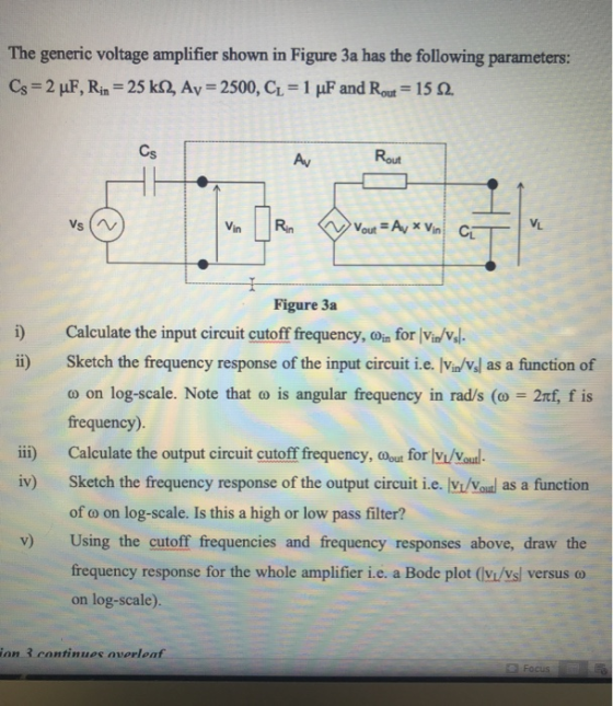
The generic voltage amplifier shown in Figure 3a has the following parameters: Cs-2μF, Rin-25 kQ, Av-2500, CL 1 μF and Rout-15 Ω Cs Rout Av Figure 3a i) Calculate the input circuit cutoff frequency, (oin or/v i) Sketch the frequency response of the input circuit ie. Ivivl as a function of ω on log-scale. Note that ω is angular frequency in rad/s (ω-2rf, f is frequency). ii) Calculate the output circuit cutoff frequency, Oout for vi/Voudl iv) Sketch the frequency response of the output circuit i.e. vi/Voul as a function of ω on log-scale. Is this a high or low pass filter? v) Using the cutoff frequencies and frequency responses above, draw the frequency response for the whole amplifier i.e. a Bode plot (︺vsl versus ω on log-scale). inn 3 continues averleaf
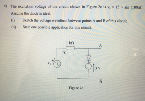
c) The excitation voltage of the circuit shown in Figure 2c is v, 15 x sin (100rt). Assume the diode is ideal (Gi) Sketch the voltage waveform between points A and B of this circuit. (i) State one possible application for this circuit 3 V Figure 2c
2. a) You have been asked to design the voltage regulator circuit shown in Figure 2b. A power supply (V.) varies from 10 V to 12 Y, and is used to power a cassette recorder. If the breakdown voltage of the Zener diode is 8 V and the cassette recorder draws a current of 10 mA when playing and 0 mA when paused, calculate: R, 40 8 V Figure 2b (i) The nominal voltage VAB. (ii) The maximum current across the Zener diode. (ii) The minimum current across the Zener diode. (iv) The variation in the voltage across AB, assuming that the Zener diode has a dynamic breakdown resistance of 5 2 A LED has been designed to emit light at a wavelength of 600 nm. Calculate the band b) gap energy (in eV) of the semiconductor material required for this device.
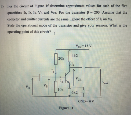
f) For the circuit of Figure 1f determine approximate values for each of the five quantities: 1, 12, 13, VB and VCE. For the transistor β-: 200, Assume that the collector and emitter currents are the same. Ignore the effect of Iz on VB. State the operational mode of the transistor and give your reasons. What is the operating point of this circuit? 20k 4k2 CE out in 10k 6k2 GND 0 V Figure 1f
b) Sketch the current - voltage characteristics for a typical silicon diode over the voltage range -2 V to +2 V. Explain how the characteristics would change if the diode was fabricated using germanium. Give an equivalent circuit representation of the device in each case. c) In a silicon diode a cument of 200 μΑ flows when a forward bias voltage of 0.5 V is applied at room temperature. Calculate the reverse saturation current of the diode. Assume that the ideality factor of the diode is 1. d) Explain briefly how an n-channel enhancement metal oxide semiconductor field effect transistor (MOSFET) operates. e) An n-channel enhancement MOSFET is used as an inverter and connected as shown in Figure le. The MOSFET has a threshold voltage VT -0.8 V and the transconductance gm (in saturation) = 2 mA / V. Design the minimum value of drain resistance Rp required to set the output voltage for logic 0 of the inverter, V, at 0.2 V 3 V RD o V Vi o V Figure le
Homework Answers
Note: According to HomeworkLib policy we have to answer for the first four parts only.thanku


Add Answer to:
A common source amplifier circuit based on a single n-channel MOSFET is shown in Figure 4b. Assume that the transconductance gm-60 mS (equivalent to mA/ V) and drain source resistance, os,...
A) For the common source amplifier below, calculate the small signal gain Av -Vo Vi (from the tra...
 Please do part a only
a) For the common source amplifier below, calculate the small signal gain Av -Vo Vi (from the transistor gate to the output node), the input resistance Rin, the output resistance Rout, and the overall voltage gain Gy Vo Vs (from the voltage source to the output node). Assume that the capacitors act as AC shorts and that the transistor's To is infinite (can be neglected) Note, you can use the small signal parameters that you...
Please do part a only
a) For the common source amplifier below, calculate the small signal gain Av -Vo Vi (from the transistor gate to the output node), the input resistance Rin, the output resistance Rout, and the overall voltage gain Gy Vo Vs (from the voltage source to the output node). Assume that the capacitors act as AC shorts and that the transistor's To is infinite (can be neglected) Note, you can use the small signal parameters that you...
4. For the amplifier in the figure below use the parameters in the table: +Vcc Re VBE- 0.7V, Ri- ...
 4. For the amplifier in the figure below use the parameters in the table: +Vcc Re VBE- 0.7V, Ri- 1002, R1-160k2, R2-320k2 R3-200k2, R6-40 k2, Rc-60k2, Vcc- 12V, Ry Do a) Draw the DC equivalent circuit and calculate the Q-point. c) Draw the AC equivalent circuit with the small signal model for the transistor. d) Calculate the voltage gain, Av-Vo/vi. Assume ro infinite. e) Draw the circuit to find the amplifier input resistance (Rin). Calculate Rin f Draw the circuit...
Q6. An amplifier circuit using an n-MOSFET is shown in Fig. Q6. The n-MOSFET has the...
 Q6. An amplifier circuit using an n-MOSFET is shown in Fig. Q6. The n-MOSFET has the following parameters: K'-1 mA/V2 and λ-0.02 w. v°' is a small signal AC voltage ource 8V 8V Vout Ra 2.56 mA Fig. Q6 (a) Calculate the DC gate voltage, Va. (b) Assuming that the n-MOSFET is operating in the saturation region and neglecting channel length modulation, calculate the threshold voltage, VrHN, given that the voltage drop across the de current sorce, Inas, has been...
Voo=5V GND V An n-channel MOSFET circuit shown in the figure is fed by a gate...
 Voo=5V GND V An n-channel MOSFET circuit shown in the figure is fed by a gate voltage Va and Vod=5V. Drain resistance Rp=2k12. The p-type substrate of the MOSFET is doped by 10" acceptor ions. The effective electron mobility in the channel when it is created is 820cm/V-s. The oxide thickness is xq=10nm with dielectric constant Ko=3.9. Also the channel length L=500nm and the depth of the device is, Z=0.4um. a. Calculate the threshold voltage to create n-channel b. Calculate...
Problem 2 Consider the feedback amplifier circuit on Figure P2. The DC current gain of transistor Q3 is -100 1. What type of feedback (or what feedback topology) do we have on the circuit in Figure P...
 Problem 2 Consider the feedback amplifier circuit on Figure P2. The DC current gain of transistor Q3 is -100 1. What type of feedback (or what feedback topology) do we have on the circuit in Figure P2? 2. Draw the A-circuit. Express and compute the open-loop voltage gain A at mid-band frequency 3, Draw the γ-circuit. Express and compute the feedback factor γ 4. Express and compute the overall gain of the feedback amplifier Ap Express and compute the input...
An amplifier circuit using a bipolar transistor is shown in Figure Q5. (a) State, with a valid re...
 An amplifier circuit using a bipolar transistor is shown in
Figure Q5.
(a) State, with a valid reason, whether this amplifier is an
emitter follower
or a common emitter configuration.
(b) Redraw Figure Q5 as a large signal equivalent circuit. Show
that:
(c) Show that the input voltage, vISAT to produce the onset of
saturation for
T1 is given by:
(d), confirm, by calculation, that
T1 is in saturation.
(e) Calculate the current in the lamp when T1 is in...
An amplifier circuit using a bipolar transistor is shown in
Figure Q5.
(a) State, with a valid reason, whether this amplifier is an
emitter follower
or a common emitter configuration.
(b) Redraw Figure Q5 as a large signal equivalent circuit. Show
that:
(c) Show that the input voltage, vISAT to produce the onset of
saturation for
T1 is given by:
(d), confirm, by calculation, that
T1 is in saturation.
(e) Calculate the current in the lamp when T1 is in...
Design a common-source MOSFET amplifier such that - Rg is a multiple of 10 - Id...
Design a common-source MOSFET amplifier such that - Rg is a multiple of 10 - Id = 0.52 mA - the amplifier input resistance is in the range of mega ohms - | Avo | = 16.7 V/V - RL = 20k - Vsig has a 2kHz frequency - Rsig = 400k, and is the input and the MOSFET has: Vt = 0.8V k = 5 mA/V^2 VA = 80 V Assume capacitors are shorted in the signal circuit and...
1. The following circuit shows a discrete common source MOSFET amplifier. The MOSFTE is n-channel MOSFET...
 1. The following circuit shows a discrete common source MOSFET amplifier. The MOSFTE is n-channel MOSFET and early voltage (Va) is c. The transconductance of the amplifier (ga) is 3 mA/V The frequency responses of the amplifier are as follows i) The three low break frequencies f 3Hz (caused by C).fiz-S0Hz (caused by Cs). fs-10Hz (caused by Ca) ii) High 3 dB frequency. f-30kHz ii) The MOSFET unity gain frequency fr-100 MHz (a) Draw small signal equivalent circuit of the...
2. For the circuit below, the n-channel enhancement MOSFET is biased to have gm-4 mA/V Find...
 2. For the circuit below, the n-channel enhancement MOSFET is biased to have gm-4 mA/V Find the mid-band voltage gain AM Design the bypass and coupling capacitors to have the three low frequency poles at 50 Hz, 10 Hz and 3 Hz, respectively. It is the rule of thumb to have a minimum total capacitance. What is the fi? If a Rs-500 Ω is inserted between the source and Cs. What the Cs should be for a same pole frequency...
A MOSFET common-source amplifier has gm=1.8mA/V, ro=100KΩ, RD=10KΩ, Cgs=2pF, Cgd=0.4pF. The amplifier is fed from a...
A MOSFET common-source amplifier has gm=1.8mA/V, ro=100KΩ, RD=10KΩ, Cgs=2pF, Cgd=0.4pF. The amplifier is fed from a voltage source with an internal resistance of 500KΩ and the output is connected to a 10KΩ load. If the lower cutoff frequency (fL) is 10KHz, find the Gain-bandwidth product of this amplifier in (dB) KHz (ignore the sign). Approximate your answer to 2 decimal point accuracy.
 Please do part a only
a) For the common source amplifier below, calculate the small signal gain Av -Vo Vi (from the transistor gate to the output node), the input resistance Rin, the output resistance Rout, and the overall voltage gain Gy Vo Vs (from the voltage source to the output node). Assume that the capacitors act as AC shorts and that the transistor's To is infinite (can be neglected) Note, you can use the small signal parameters that you...
Please do part a only
a) For the common source amplifier below, calculate the small signal gain Av -Vo Vi (from the transistor gate to the output node), the input resistance Rin, the output resistance Rout, and the overall voltage gain Gy Vo Vs (from the voltage source to the output node). Assume that the capacitors act as AC shorts and that the transistor's To is infinite (can be neglected) Note, you can use the small signal parameters that you...
 4. For the amplifier in the figure below use the parameters in the table: +Vcc Re VBE- 0.7V, Ri- 1002, R1-160k2, R2-320k2 R3-200k2, R6-40 k2, Rc-60k2, Vcc- 12V, Ry Do a) Draw the DC equivalent circuit and calculate the Q-point. c) Draw the AC equivalent circuit with the small signal model for the transistor. d) Calculate the voltage gain, Av-Vo/vi. Assume ro infinite. e) Draw the circuit to find the amplifier input resistance (Rin). Calculate Rin f Draw the circuit...
 Q6. An amplifier circuit using an n-MOSFET is shown in Fig. Q6. The n-MOSFET has the following parameters: K'-1 mA/V2 and λ-0.02 w. v°' is a small signal AC voltage ource 8V 8V Vout Ra 2.56 mA Fig. Q6 (a) Calculate the DC gate voltage, Va. (b) Assuming that the n-MOSFET is operating in the saturation region and neglecting channel length modulation, calculate the threshold voltage, VrHN, given that the voltage drop across the de current sorce, Inas, has been...
 Voo=5V GND V An n-channel MOSFET circuit shown in the figure is fed by a gate voltage Va and Vod=5V. Drain resistance Rp=2k12. The p-type substrate of the MOSFET is doped by 10" acceptor ions. The effective electron mobility in the channel when it is created is 820cm/V-s. The oxide thickness is xq=10nm with dielectric constant Ko=3.9. Also the channel length L=500nm and the depth of the device is, Z=0.4um. a. Calculate the threshold voltage to create n-channel b. Calculate...
 Problem 2 Consider the feedback amplifier circuit on Figure P2. The DC current gain of transistor Q3 is -100 1. What type of feedback (or what feedback topology) do we have on the circuit in Figure P2? 2. Draw the A-circuit. Express and compute the open-loop voltage gain A at mid-band frequency 3, Draw the γ-circuit. Express and compute the feedback factor γ 4. Express and compute the overall gain of the feedback amplifier Ap Express and compute the input...
 An amplifier circuit using a bipolar transistor is shown in
Figure Q5.
(a) State, with a valid reason, whether this amplifier is an
emitter follower
or a common emitter configuration.
(b) Redraw Figure Q5 as a large signal equivalent circuit. Show
that:
(c) Show that the input voltage, vISAT to produce the onset of
saturation for
T1 is given by:
(d), confirm, by calculation, that
T1 is in saturation.
(e) Calculate the current in the lamp when T1 is in...
An amplifier circuit using a bipolar transistor is shown in
Figure Q5.
(a) State, with a valid reason, whether this amplifier is an
emitter follower
or a common emitter configuration.
(b) Redraw Figure Q5 as a large signal equivalent circuit. Show
that:
(c) Show that the input voltage, vISAT to produce the onset of
saturation for
T1 is given by:
(d), confirm, by calculation, that
T1 is in saturation.
(e) Calculate the current in the lamp when T1 is in...
 1. The following circuit shows a discrete common source MOSFET amplifier. The MOSFTE is n-channel MOSFET and early voltage (Va) is c. The transconductance of the amplifier (ga) is 3 mA/V The frequency responses of the amplifier are as follows i) The three low break frequencies f 3Hz (caused by C).fiz-S0Hz (caused by Cs). fs-10Hz (caused by Ca) ii) High 3 dB frequency. f-30kHz ii) The MOSFET unity gain frequency fr-100 MHz (a) Draw small signal equivalent circuit of the...
 2. For the circuit below, the n-channel enhancement MOSFET is biased to have gm-4 mA/V Find the mid-band voltage gain AM Design the bypass and coupling capacitors to have the three low frequency poles at 50 Hz, 10 Hz and 3 Hz, respectively. It is the rule of thumb to have a minimum total capacitance. What is the fi? If a Rs-500 Ω is inserted between the source and Cs. What the Cs should be for a same pole frequency...
Most questions answered within 3 hours.
-
At 1 bar, how much energy is required to heat 61.0 g of H2O(s)
at −12.0...
asked 13 minutes ago -
Find the mixed-strategy equilibrium to the Battle of the sexes
game in Figure 5.1 below
Hockey...
asked 15 minutes ago -
Use the following information to answer the next three
questions.
QUESTION 5
As of today, the...
asked 20 minutes ago -
Using the specific identification method: Date Units purchased
Cost per unit Ending inventory March 1 15...
asked 23 minutes ago -
PLEASE HELP, NO ONE IS ANSWERING MY QUESTION AND IT IS SUE TODAY
WORTH 20% OF...
asked 37 minutes ago -
α = 0.0007889 T, I = 2.9 A
Other Magnetic Fields: First, based on your
value...
asked 37 minutes ago -
This assignment is a continuation of the 2nd one. You as a HR
Manager, select an...
asked 39 minutes ago -
Hastings Entertainment has a beta of 0.64. If the market return
is expected to be 13.80...
asked 51 minutes ago -
9. Depository institutions are always:
a. illiquid
b. profitable
c. insolvent
d. all of the above...
asked 59 minutes ago -
Use AstroTurf Company's income statement below to answer the
following two questions. Answer these questions with...
asked 59 minutes ago -
How is a firm's task
environment different from its general environment? Provide
examples of both types...
asked 57 minutes ago -
What is one reason Innovators can adopt innovations so
early?
Group of answer choices
they are...
asked 59 minutes ago