

Homework Answers


Add Answer to:
Q5. Consider the circuit in Fig.1 (right). Assume 9m, 9o, VT, W, L, Mn, and Cox...
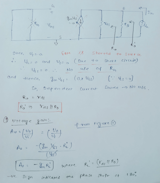
Rsig Nahyan vgs ( gmugs, r01 RDS Vsig ) Ril Consider the small signal equivalent circuit...
 Rsig Nahyan vgs ( gmugs, r01 RDS Vsig ) Ril Consider the small signal equivalent circuit of an amplifier shown above. The parameters are given to be: R1 = 3000, R2 = 10160, R2=100%, RD=RL=50 Rsig = 202, VGS1=3.5V. Vt = 0.5V and kn = 1mA/V^2. The transistor output resistances are represented by ro1, ra2 with both the transistors in saturation and having |MAL= 40V and same DC current flowing through them Find the small signal parameter of the MOSFET:...
Q6. An amplifier circuit using an n-MOSFET is shown in Fig. Q6. The n-MOSFET has the...
 Q6. An amplifier circuit using an n-MOSFET is shown in Fig. Q6. The n-MOSFET has the following parameters: K'-1 mA/V2 and λ-0.02 w. v°' is a small signal AC voltage ource 8V 8V Vout Ra 2.56 mA Fig. Q6 (a) Calculate the DC gate voltage, Va. (b) Assuming that the n-MOSFET is operating in the saturation region and neglecting channel length modulation, calculate the threshold voltage, VrHN, given that the voltage drop across the de current sorce, Inas, has been...
An analogue amplifier circuit is shown in Figure 1 below. VDD Q5 15V JL - Vout...
 An analogue amplifier circuit is shown in Figure 1 below. VDD Q5 15V JL - Vout Irer RI Vina JET T7T Figure 1 Integrated amplifier circuit. Circuit Data: Vpp = 15 V, IREF = I1 = I2 = 1.0 mA Transistor Data: Q1: NMOS, un Cox = 80 A/V?, W/L = 100 um/0.8 um, Vtn = 0.8 V, L = 0.10 um/V Q2: NPN BJT, B = 100, Vbe = 0.7 V, VA = 150 V Q3, Q4: NMOS, un...
6.108 (d) Section 6.5: Discrete-Circuit Amplifiers 6.107 Calculate overall voltage gain G, of a 3 mA/V, ro= = 1...
 6.108 (d)
Section 6.5: Discrete-Circuit Amplifiers 6.107 Calculate overall voltage gain G, of a 3 mA/V, ro= = 10 MS2. The amplifier is the common-source amplifier for which g 100 k2, RD 10 k2, and RG fed from a signal source with a Thevenin resistance of l M2, and the amplifier output is coupled of 20 k2 to a load resistance SIM 6.108 The NMOS transistor in the CS amplifier shown in Fig. P6.108 has V, = 0.7 V and...
6.108 (d)
Section 6.5: Discrete-Circuit Amplifiers 6.107 Calculate overall voltage gain G, of a 3 mA/V, ro= = 10 MS2. The amplifier is the common-source amplifier for which g 100 k2, RD 10 k2, and RG fed from a signal source with a Thevenin resistance of l M2, and the amplifier output is coupled of 20 k2 to a load resistance SIM 6.108 The NMOS transistor in the CS amplifier shown in Fig. P6.108 has V, = 0.7 V and...
Q1. For the cascade amplifier circuit shown in Fig (1): a) What are the functions of the capacitors C, C2 and C3? And w...
 Q1. For the cascade amplifier circuit shown in Fig (1): a) What are the functions of the capacitors C, C2 and C3? And what are the functions of the capacitors Cs and CE? b) What are the functions of the resistors RD and Rc? c) Draw the DC biasing circuits for each stage. d) Find loa, VGsa, VDs and gm for the JFET stage (you may use either mathematical or graphical methods) e) Calculate l, Ic, le and Ve for...
A common source amplifier circuit based on a single n-channel MOSFET is shown in Figure 4b. Assume that the transconductance gm-60 mS (equivalent to mA/ V) and drain source resistance, os,...
 A common source amplifier circuit based on a single n-channel MOSFET is shown in Figure 4b. Assume that the transconductance gm-60 mS (equivalent to mA/ V) and drain source resistance, os, is so large it may be neglected. 0) Calculate the open circuit voltage gain Av Yout/ Vis. i) The amplifier has a load of 10 k2. Determine the current gain Va. = 12 V 150k 4k3 Vout Vin 200k GND = 0 V Figure 4b a) State the name...
Problem 3: Design Problem On Figure P3a, you have a Common Source (CS) n-channel MOSFET amplifier....
 Problem 3: Design Problem On Figure P3a, you have a Common Source (CS) n-channel MOSFET amplifier. Notice the absence of a source resistor Rsig and load resistor R. If we know how the present amplifier (the one on Figure P3a) behaves without Rsig and RL, we can infer its behaviors if Rsig and R were to be added. design the amplifier circuit on Figure P3a, i.e., you have to find appropriate values for RGj You are to RG,, RD, and...
 Rsig Nahyan vgs ( gmugs, r01 RDS Vsig ) Ril Consider the small signal equivalent circuit of an amplifier shown above. The parameters are given to be: R1 = 3000, R2 = 10160, R2=100%, RD=RL=50 Rsig = 202, VGS1=3.5V. Vt = 0.5V and kn = 1mA/V^2. The transistor output resistances are represented by ro1, ra2 with both the transistors in saturation and having |MAL= 40V and same DC current flowing through them Find the small signal parameter of the MOSFET:...
 Q6. An amplifier circuit using an n-MOSFET is shown in Fig. Q6. The n-MOSFET has the following parameters: K'-1 mA/V2 and λ-0.02 w. v°' is a small signal AC voltage ource 8V 8V Vout Ra 2.56 mA Fig. Q6 (a) Calculate the DC gate voltage, Va. (b) Assuming that the n-MOSFET is operating in the saturation region and neglecting channel length modulation, calculate the threshold voltage, VrHN, given that the voltage drop across the de current sorce, Inas, has been...
 An analogue amplifier circuit is shown in Figure 1 below. VDD Q5 15V JL - Vout Irer RI Vina JET T7T Figure 1 Integrated amplifier circuit. Circuit Data: Vpp = 15 V, IREF = I1 = I2 = 1.0 mA Transistor Data: Q1: NMOS, un Cox = 80 A/V?, W/L = 100 um/0.8 um, Vtn = 0.8 V, L = 0.10 um/V Q2: NPN BJT, B = 100, Vbe = 0.7 V, VA = 150 V Q3, Q4: NMOS, un...
 6.108 (d)
Section 6.5: Discrete-Circuit Amplifiers 6.107 Calculate overall voltage gain G, of a 3 mA/V, ro= = 10 MS2. The amplifier is the common-source amplifier for which g 100 k2, RD 10 k2, and RG fed from a signal source with a Thevenin resistance of l M2, and the amplifier output is coupled of 20 k2 to a load resistance SIM 6.108 The NMOS transistor in the CS amplifier shown in Fig. P6.108 has V, = 0.7 V and...
6.108 (d)
Section 6.5: Discrete-Circuit Amplifiers 6.107 Calculate overall voltage gain G, of a 3 mA/V, ro= = 10 MS2. The amplifier is the common-source amplifier for which g 100 k2, RD 10 k2, and RG fed from a signal source with a Thevenin resistance of l M2, and the amplifier output is coupled of 20 k2 to a load resistance SIM 6.108 The NMOS transistor in the CS amplifier shown in Fig. P6.108 has V, = 0.7 V and...
 Q1. For the cascade amplifier circuit shown in Fig (1): a) What are the functions of the capacitors C, C2 and C3? And what are the functions of the capacitors Cs and CE? b) What are the functions of the resistors RD and Rc? c) Draw the DC biasing circuits for each stage. d) Find loa, VGsa, VDs and gm for the JFET stage (you may use either mathematical or graphical methods) e) Calculate l, Ic, le and Ve for...
 A common source amplifier circuit based on a single n-channel MOSFET is shown in Figure 4b. Assume that the transconductance gm-60 mS (equivalent to mA/ V) and drain source resistance, os, is so large it may be neglected. 0) Calculate the open circuit voltage gain Av Yout/ Vis. i) The amplifier has a load of 10 k2. Determine the current gain Va. = 12 V 150k 4k3 Vout Vin 200k GND = 0 V Figure 4b a) State the name...
 Problem 3: Design Problem On Figure P3a, you have a Common Source (CS) n-channel MOSFET amplifier. Notice the absence of a source resistor Rsig and load resistor R. If we know how the present amplifier (the one on Figure P3a) behaves without Rsig and RL, we can infer its behaviors if Rsig and R were to be added. design the amplifier circuit on Figure P3a, i.e., you have to find appropriate values for RGj You are to RG,, RD, and...
Most questions answered within 3 hours.
-
284 mL of a 0.52 M potassium hydroxide solution is added to 467
mL of a...
asked 18 minutes ago -
exercise on VSEPR and molecular structrue.
octahedral
SeCl62-
TeCl62-
ClF62-
distorted
SeF62–
IF6–
asked 19 minutes ago -
Little’s Law: Val d’Costa is a world famous ski village in the
French Alps. Because of...
asked 1 hour ago -
Find the absolute error D for the calculation if A + B/C=D A=
9.4 +/- 0.4...
asked 1 hour ago -
New Air Heating and Cooling, manufactures furnaces and central
air units. The company pride itself on...
asked 1 hour ago -
A coach uses a new technique to train gymnasts. Seven
gymnasts were randomly selected and their...
asked 3 hours ago -
While rotating the tires on your car you notice a rock [mass =
0.1 Kg] stuck...
asked 5 hours ago -
Using MARS simulator, write MIPS programs according to
the following scenarios: Receive a positive integer number...
asked 7 hours ago -
An object in front of a concave mirror has a real image that is
11.5 cm...
asked 7 hours ago -
Consider the reaction, C3 H8 + O2 --> CO2 + H2O. How many
moles of O2...
asked 9 hours ago -
You and your opponent both roll a fair die. If you both roll the
same number,...
asked 9 hours ago -
In a study of the accuracy of fast food drive-through orders,
Restaurant A had 257 accurate...
asked 9 hours ago