
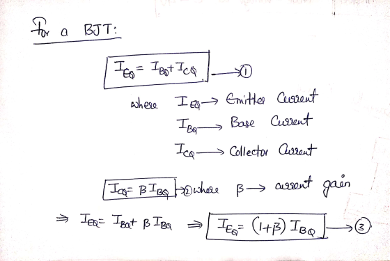
Homework Answers


Add Answer to:
Design a transistor biasing circuit as shown below. Assume ß = 100, Ice = 10 mA,...
Q. 3. Design a transistor biasing circuit as shown below. Assume ß = 100, lco =...
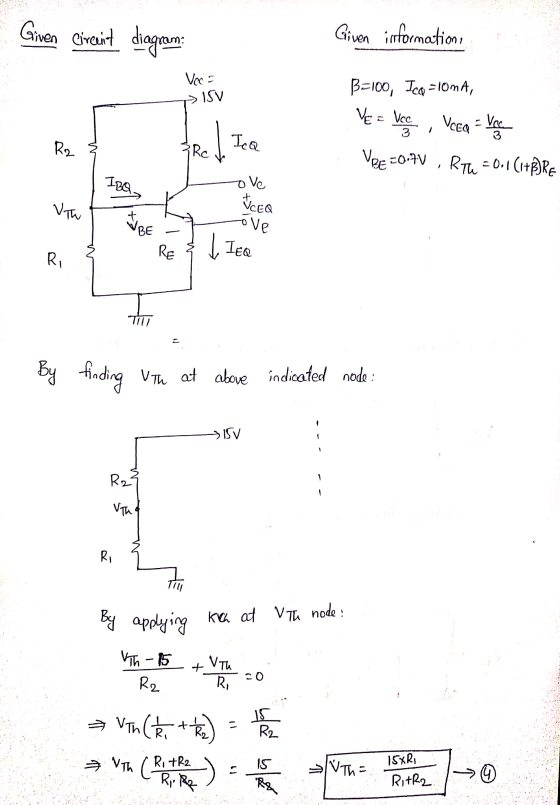
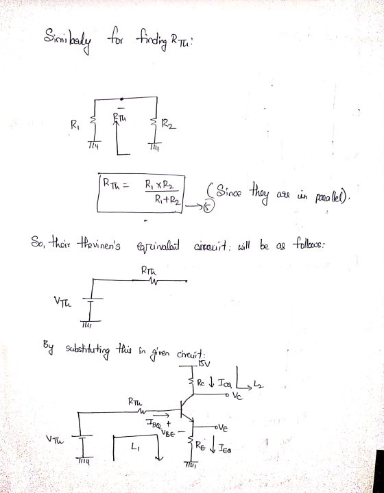
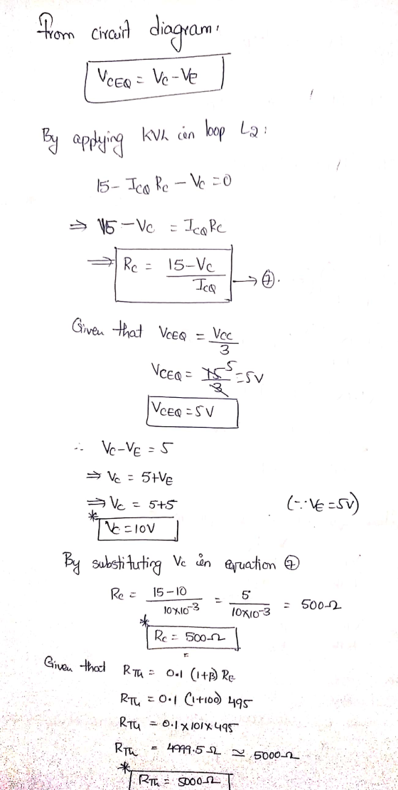
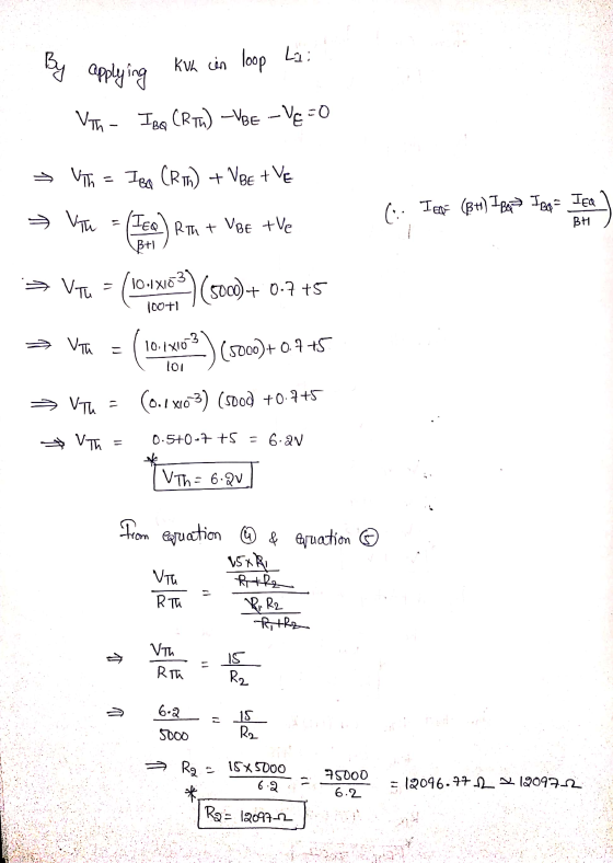
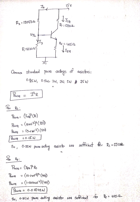
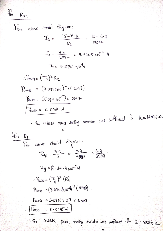
 Q. 3. Design a transistor biasing circuit as shown below. Assume ß = 100, lco = 10 mA, VE = Vcc/3, VCEQ = Vcc/3 and VBE = 0.7 V. RTH = 0.1 (1 + B)RE . Also find the power rating of all resistors. +15V R2 Rc V10 R1 RE
Q. 3. Design a transistor biasing circuit as shown below. Assume B = 100, Ica =...
 Q. 3. Design a transistor biasing circuit as shown below. Assume B = 100, Ica = 10 mA, VE = Vcc/3, VceQ = Vcc /3 and VBE = 0.7 V. RTH = 0.1 (1 + B)RE . Also find the power rating of all resistors. (25) > +15V R2 Rc Vio R1 RE
RE 3K30 V_B Dar v.ce vor RC ROOLIVC B = 100 and VBE = -0.7V Fig....
 RE 3K30 V_B Dar v.ce vor RC ROOLIVC B = 100 and VBE = -0.7V Fig. 2 1. Calculate: VB.Ve V, and Vce. 2. Calculate:IB., and Ic. 3. Using the same circuit and assuming active mode operation, find the resistor values (R1, R2, Re and Rc), to bias the transistor at the Q-point: Vce = -8 V and Ic = 8 mA. Use the following parameters: Vcc = 20 V,ß = 200,Ve = 16 V, RTH = 0.1BRg.
The 1 mA. V, ls -VE -15 15 V, in the following differential amplifier circuit, Vcc parameters are given as β, 100, VBE# 0.7 V, pr-25 mV, K.-100 V. transistor Rc-10 kΩ For: RE-150 Ω Rc Rc REE-200...
 The 1 mA. V, ls -VE -15 15 V, in the following differential amplifier circuit, Vcc parameters are given as β, 100, VBE# 0.7 V, pr-25 mV, K.-100 V. transistor Rc-10 kΩ For: RE-150 Ω Rc Rc REE-200 kΩ a) What is the input differential resistance, Rid b) What is the overall voltage gain vV? You c) What is input common mode resistance, d) What is the worst case common mode gain that appear across the two input terminals? (4...
design a Voltage Divider Circuit that has the following – VCC= 12 V IC=2.5 mA ...
design a Voltage Divider Circuit that has the following – VCC= 12 V IC=2.5 mA VCE = 6 V For the design, you will use a 2n3904 npn transistor. Assume a β of 150. Determine values for RC, RE, R1, and R2
Consider the BJT common-emitter amplifier in Figure 1. Assume that the 2N3904G transistor has the following parameters: β-206, VBE-0.TV and the Early voltage VAT 1000V. vCC RB1a I multiple resistors...
 Consider the BJT common-emitter amplifier in Figure 1. Assume that the 2N3904G transistor has the following parameters: β-206, VBE-0.TV and the Early voltage VAT 1000V. vCC RB1a I multiple resistors RC want n Vload 22HF Rload 01 2N3904G V1 6302 4.7HF RE2CE 0.01Vpk 1kHz maliple esistons lue you available in the ki Figure 1 BJT CE amplifier 0.5 V and VC-3 V (a) Design the DC biasing circuit so that lc-2 mA, VCE = 2.5 V, VE
Consider the BJT...
Consider the BJT common-emitter amplifier in Figure 1. Assume that the 2N3904G transistor has the following parameters: β-206, VBE-0.TV and the Early voltage VAT 1000V. vCC RB1a I multiple resistors RC want n Vload 22HF Rload 01 2N3904G V1 6302 4.7HF RE2CE 0.01Vpk 1kHz maliple esistons lue you available in the ki Figure 1 BJT CE amplifier 0.5 V and VC-3 V (a) Design the DC biasing circuit so that lc-2 mA, VCE = 2.5 V, VE
Consider the BJT...
results to verify your design. 2. For the circuit in Figure 2 calculate and select standard...
 results to verify your design. 2. For the circuit in Figure 2 calculate and select standard value resistors for R1, R2, Rc and RE So that Vc= .5*Vcc volts and Ic = 1.0 mA (± 10%) X Photos -figure 2.PNG RC ŞRb1 2N3904 15V _ SRb2 SRE Figure 2: Common Emitter Stiff Bias Reference Circuit
For the circuit shown below, let B = 100 and VBE = 0.7 V. (a) Find...
 For the circuit shown below, let B = 100 and VBE = 0.7 V. (a) Find VTH and RTH for the base circuit. (b) Determine Ica and VCEQ + 5V +15V 500 ΚΩ 50 ΚΩ + 3V 500 ΚΩ 70 ΚΩ 5 ΚΩ 1. 5V .5V
(2+5 pts) Consider the bias circuit below for a transistor amplifier designed for active region operation....
 (2+5 pts) Consider the bias circuit below for a transistor amplifier designed for active region operation. The desired bias point parameters are lg = 3 mA and Ic = 2.97 mA. Assume VBE- 0.7 V and VT=25 mV. Determine the emitter voltage VE . Choose the best answer. VCC +15 V Vc RBB VB LVE V BB RE 500 S2 1.49 V O2v 01.5V O 0.7V
Problem 4 (20 %) For the circuit shown in Figure 4 determine IB, IC, and VC....
 Problem 4 (20 %) For the circuit shown in Figure 4 determine IB,
IC, and VC. Data VCC=9 V VBB=4 V R2= 165 k R1= 2.5 k Transistor
Assume VBE ≈ 0.7 V and =150
Derive all the results. Give the answers with the preestablished
prefix.
FAVOR DIBUJAR LOS CIRCUITOS
Problem 4 (206) For the circuit shown in Figure 4 determine IB, I, and Vc. Data Ve=9 V V=4V R = 165 kg R=2.5k_2 Transistor Assume VE 0.7 V and...
Problem 4 (20 %) For the circuit shown in Figure 4 determine IB,
IC, and VC. Data VCC=9 V VBB=4 V R2= 165 k R1= 2.5 k Transistor
Assume VBE ≈ 0.7 V and =150
Derive all the results. Give the answers with the preestablished
prefix.
FAVOR DIBUJAR LOS CIRCUITOS
Problem 4 (206) For the circuit shown in Figure 4 determine IB, I, and Vc. Data Ve=9 V V=4V R = 165 kg R=2.5k_2 Transistor Assume VE 0.7 V and...
 Q. 3. Design a transistor biasing circuit as shown below. Assume ß = 100, lco = 10 mA, VE = Vcc/3, VCEQ = Vcc/3 and VBE = 0.7 V. RTH = 0.1 (1 + B)RE . Also find the power rating of all resistors. +15V R2 Rc V10 R1 RE
 Q. 3. Design a transistor biasing circuit as shown below. Assume B = 100, Ica = 10 mA, VE = Vcc/3, VceQ = Vcc /3 and VBE = 0.7 V. RTH = 0.1 (1 + B)RE . Also find the power rating of all resistors. (25) > +15V R2 Rc Vio R1 RE
 RE 3K30 V_B Dar v.ce vor RC ROOLIVC B = 100 and VBE = -0.7V Fig. 2 1. Calculate: VB.Ve V, and Vce. 2. Calculate:IB., and Ic. 3. Using the same circuit and assuming active mode operation, find the resistor values (R1, R2, Re and Rc), to bias the transistor at the Q-point: Vce = -8 V and Ic = 8 mA. Use the following parameters: Vcc = 20 V,ß = 200,Ve = 16 V, RTH = 0.1BRg.
 The 1 mA. V, ls -VE -15 15 V, in the following differential amplifier circuit, Vcc parameters are given as β, 100, VBE# 0.7 V, pr-25 mV, K.-100 V. transistor Rc-10 kΩ For: RE-150 Ω Rc Rc REE-200 kΩ a) What is the input differential resistance, Rid b) What is the overall voltage gain vV? You c) What is input common mode resistance, d) What is the worst case common mode gain that appear across the two input terminals? (4...
 Consider the BJT common-emitter amplifier in Figure 1. Assume that the 2N3904G transistor has the following parameters: β-206, VBE-0.TV and the Early voltage VAT 1000V. vCC RB1a I multiple resistors RC want n Vload 22HF Rload 01 2N3904G V1 6302 4.7HF RE2CE 0.01Vpk 1kHz maliple esistons lue you available in the ki Figure 1 BJT CE amplifier 0.5 V and VC-3 V (a) Design the DC biasing circuit so that lc-2 mA, VCE = 2.5 V, VE
Consider the BJT...
Consider the BJT common-emitter amplifier in Figure 1. Assume that the 2N3904G transistor has the following parameters: β-206, VBE-0.TV and the Early voltage VAT 1000V. vCC RB1a I multiple resistors RC want n Vload 22HF Rload 01 2N3904G V1 6302 4.7HF RE2CE 0.01Vpk 1kHz maliple esistons lue you available in the ki Figure 1 BJT CE amplifier 0.5 V and VC-3 V (a) Design the DC biasing circuit so that lc-2 mA, VCE = 2.5 V, VE
Consider the BJT...
 results to verify your design. 2. For the circuit in Figure 2 calculate and select standard value resistors for R1, R2, Rc and RE So that Vc= .5*Vcc volts and Ic = 1.0 mA (± 10%) X Photos -figure 2.PNG RC ŞRb1 2N3904 15V _ SRb2 SRE Figure 2: Common Emitter Stiff Bias Reference Circuit
 For the circuit shown below, let B = 100 and VBE = 0.7 V. (a) Find VTH and RTH for the base circuit. (b) Determine Ica and VCEQ + 5V +15V 500 ΚΩ 50 ΚΩ + 3V 500 ΚΩ 70 ΚΩ 5 ΚΩ 1. 5V .5V
 (2+5 pts) Consider the bias circuit below for a transistor amplifier designed for active region operation. The desired bias point parameters are lg = 3 mA and Ic = 2.97 mA. Assume VBE- 0.7 V and VT=25 mV. Determine the emitter voltage VE . Choose the best answer. VCC +15 V Vc RBB VB LVE V BB RE 500 S2 1.49 V O2v 01.5V O 0.7V
 Problem 4 (20 %) For the circuit shown in Figure 4 determine IB,
IC, and VC. Data VCC=9 V VBB=4 V R2= 165 k R1= 2.5 k Transistor
Assume VBE ≈ 0.7 V and =150
Derive all the results. Give the answers with the preestablished
prefix.
FAVOR DIBUJAR LOS CIRCUITOS
Problem 4 (206) For the circuit shown in Figure 4 determine IB, I, and Vc. Data Ve=9 V V=4V R = 165 kg R=2.5k_2 Transistor Assume VE 0.7 V and...
Problem 4 (20 %) For the circuit shown in Figure 4 determine IB,
IC, and VC. Data VCC=9 V VBB=4 V R2= 165 k R1= 2.5 k Transistor
Assume VBE ≈ 0.7 V and =150
Derive all the results. Give the answers with the preestablished
prefix.
FAVOR DIBUJAR LOS CIRCUITOS
Problem 4 (206) For the circuit shown in Figure 4 determine IB, I, and Vc. Data Ve=9 V V=4V R = 165 kg R=2.5k_2 Transistor Assume VE 0.7 V and...
Most questions answered within 3 hours.
-
A sample of 45 observations is selected from a normal
population. The sample mean is 49,...
asked 23 seconds ago -
A firm operating in a purely competitive environment is faced
with a market price of $250....
asked 4 minutes ago -
•Let’s say someone claims the average population size is
600 feet squared and the housing authority...
asked 11 minutes ago -
Cynaide is a deadly poison that blocks the last step in the
electron transport chain of...
asked 16 minutes ago -
Your friend tells you that there is a vending machine on campus
that dispenses M&M packs...
asked 31 minutes ago -
What advantages are there to using piperidine rather than
hydroxide as a base?
asked 29 minutes ago -
7. The life of a Freeze Breeze electric fan is normally
distributed with a mean 4...
asked 32 minutes ago -
1. A 751 mL NaCl solution is diluted to a volume of 1.06 L and a...
asked 37 minutes ago -
8
A $20,000 face value STRIPS is currently quoted at 38.642 and
has 8 years to...
asked 38 minutes ago -
The current exchange rate between the Japanese yen and
the US dollar is 120 yen per...
asked 40 minutes ago -
Marla’s Massages and More bought a special massage table two
years ago for $9,300. At the...
asked 47 minutes ago -
Suppose you require a peak output voltage of 15.0 V and have
available an AC source...
asked 47 minutes ago