
Homework Answers


Design a transistor biasing circuit as shown below. Assume ß = 100, Ice = 10 mA,...
 Design a transistor biasing circuit as shown below. Assume ß = 100, Ice = 10 mA, VE = Vcc/3, VCEQ = Vcc/3 and VBE = 0.7 V. RTH = 0.1 (1 + BRE. Also find the power rating of all resistors. +15V R2 Rc V 10 R1 RE
Q. 3. Design a transistor biasing circuit as shown below. Assume ß = 100, lco =...
 Q. 3. Design a transistor biasing circuit as shown below. Assume ß = 100, lco = 10 mA, VE = Vcc/3, VCEQ = Vcc/3 and VBE = 0.7 V. RTH = 0.1 (1 + B)RE . Also find the power rating of all resistors. +15V R2 Rc V10 R1 RE
Q. 3. Design a transistor biasing circuit as shown below. Assume B = 100, Ica =...
 Q. 3. Design a transistor biasing circuit as shown below. Assume B = 100, Ica = 10 mA, VE = Vcc/3, VceQ = Vcc /3 and VBE = 0.7 V. RTH = 0.1 (1 + B)RE . Also find the power rating of all resistors. (25) > +15V R2 Rc Vio R1 RE
The 1 mA. V, ls -VE -15 15 V, in the following differential amplifier circuit, Vcc parameters are given as β, 100, VBE# 0.7 V, pr-25 mV, K.-100 V. transistor Rc-10 kΩ For: RE-150 Ω Rc Rc REE-200...
 The 1 mA. V, ls -VE -15 15 V, in the following differential amplifier circuit, Vcc parameters are given as β, 100, VBE# 0.7 V, pr-25 mV, K.-100 V. transistor Rc-10 kΩ For: RE-150 Ω Rc Rc REE-200 kΩ a) What is the input differential resistance, Rid b) What is the overall voltage gain vV? You c) What is input common mode resistance, d) What is the worst case common mode gain that appear across the two input terminals? (4...
RE -3.3k2 Figure 5. Vbe-0.7V (active), Vce 0.2V (saturation), p-100 For the circuit shown in Figure...
 RE -3.3k2 Figure 5. Vbe-0.7V (active), Vce 0.2V (saturation), p-100 For the circuit shown in Figure 5: a) If V oV DC, find the DC bias point for Q1? b) Draw the small signal equivalent circuit and evaluate the small signal AC voltage gain. c) Sketch le vs Vce and show the operating point for the transistor. d) How would you change the bias to obtain maximum signal swing?
(2+5 pts) Consider the bias circuit below for a transistor amplifier designed for active region operation....
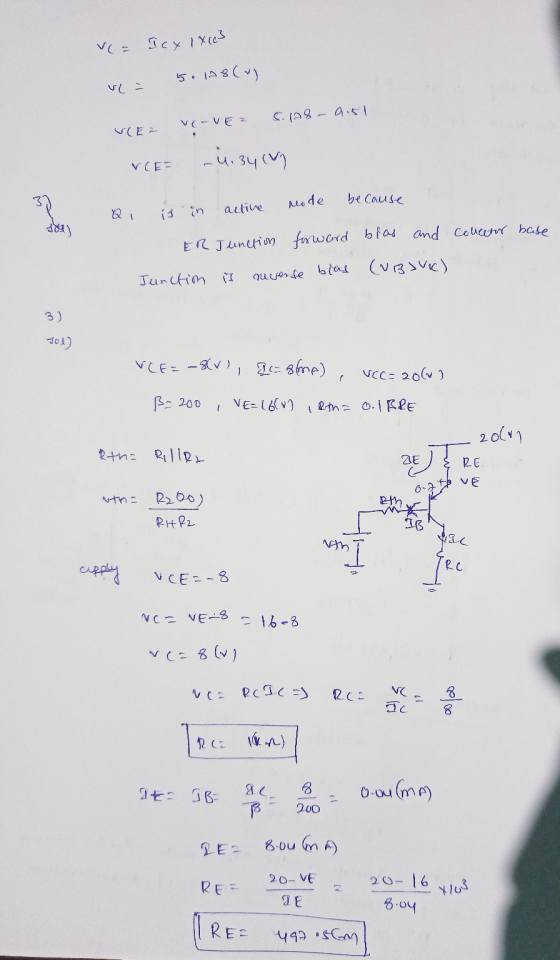
 (2+5 pts) Consider the bias circuit below for a transistor amplifier designed for active region operation. The desired bias point parameters are lg = 3 mA and Ic = 2.97 mA. Assume VBE- 0.7 V and VT=25 mV. Determine the emitter voltage VE . Choose the best answer. VCC +15 V Vc RBB VB LVE V BB RE 500 S2 1.49 V O2v 01.5V O 0.7V
Experiment 2: Good biasing Set up the circuit with R2 12 k2, R RE 1 k, and Vcc 15 V 39 k2, Rc = 2 k?. Circuit An...
 Experiment 2: Good biasing Set up the circuit with R2 12 k2, R RE 1 k, and Vcc 15 V 39 k2, Rc = 2 k?. Circuit Analysis: Compute Ic, I, and VCE PSpice Simulation: a) Simulate the circuit with PSpice (bias point details only) and compare values of Ic, IB, VCE, and VBE from PSpice simulations with your analytical calculations. b) Rerun your PSpice simulations for temperatures of 0 and 60°C. Make a table of Ic IB, VCE, and...
Question 1 (4 points) Voc 3 Rc RB13 The voltage-divider bias circuit shown has Rc =...
 Question 1 (4 points) Voc 3 Rc RB13 The voltage-divider bias circuit shown has Rc = 2 k12, RE = 400 12, RB1 = 300 k22, RB2 = 100 ks and Vcc = 25 V. Assume that VBE = 0.7 V and B = 90. Determine the Q- point (Ic and VCE) for the bias circuit. OVCE = 5.91 V Ic = 3.09 mA OVCE = 12.07 V Ic = 2.40 mA O VCE = 14.22 V Ic = 4.48...
4. For the amplifier in the figure below use the parameters in the table: +Vcc Re VBE- 0.7V, Ri- ...
 4. For the amplifier in the figure below use the parameters in the table: +Vcc Re VBE- 0.7V, Ri- 1002, R1-160k2, R2-320k2 R3-200k2, R6-40 k2, Rc-60k2, Vcc- 12V, Ry Do a) Draw the DC equivalent circuit and calculate the Q-point. c) Draw the AC equivalent circuit with the small signal model for the transistor. d) Calculate the voltage gain, Av-Vo/vi. Assume ro infinite. e) Draw the circuit to find the amplifier input resistance (Rin). Calculate Rin f Draw the circuit...
In the following problem. Vcc =9.3 v. 1g=0.6 mA, R1=2.9 ko, R2= 6.6 k0. Assume B=58...
 In the following problem. Vcc =9.3 v. 1g=0.6 mA, R1=2.9 ko, R2= 6.6 k0. Assume B=58 and VBE=0.7V Find the operating point for each transistor (VCE, IC) In the answer box, write Ic3 only 30kn OB ER Η 1kΩΣ 80ks Riš 3kn -Vcc
 Design a transistor biasing circuit as shown below. Assume ß = 100, Ice = 10 mA, VE = Vcc/3, VCEQ = Vcc/3 and VBE = 0.7 V. RTH = 0.1 (1 + BRE. Also find the power rating of all resistors. +15V R2 Rc V 10 R1 RE
 Q. 3. Design a transistor biasing circuit as shown below. Assume ß = 100, lco = 10 mA, VE = Vcc/3, VCEQ = Vcc/3 and VBE = 0.7 V. RTH = 0.1 (1 + B)RE . Also find the power rating of all resistors. +15V R2 Rc V10 R1 RE
 Q. 3. Design a transistor biasing circuit as shown below. Assume B = 100, Ica = 10 mA, VE = Vcc/3, VceQ = Vcc /3 and VBE = 0.7 V. RTH = 0.1 (1 + B)RE . Also find the power rating of all resistors. (25) > +15V R2 Rc Vio R1 RE
 The 1 mA. V, ls -VE -15 15 V, in the following differential amplifier circuit, Vcc parameters are given as β, 100, VBE# 0.7 V, pr-25 mV, K.-100 V. transistor Rc-10 kΩ For: RE-150 Ω Rc Rc REE-200 kΩ a) What is the input differential resistance, Rid b) What is the overall voltage gain vV? You c) What is input common mode resistance, d) What is the worst case common mode gain that appear across the two input terminals? (4...
 RE -3.3k2 Figure 5. Vbe-0.7V (active), Vce 0.2V (saturation), p-100 For the circuit shown in Figure 5: a) If V oV DC, find the DC bias point for Q1? b) Draw the small signal equivalent circuit and evaluate the small signal AC voltage gain. c) Sketch le vs Vce and show the operating point for the transistor. d) How would you change the bias to obtain maximum signal swing?
 (2+5 pts) Consider the bias circuit below for a transistor amplifier designed for active region operation. The desired bias point parameters are lg = 3 mA and Ic = 2.97 mA. Assume VBE- 0.7 V and VT=25 mV. Determine the emitter voltage VE . Choose the best answer. VCC +15 V Vc RBB VB LVE V BB RE 500 S2 1.49 V O2v 01.5V O 0.7V
 Experiment 2: Good biasing Set up the circuit with R2 12 k2, R RE 1 k, and Vcc 15 V 39 k2, Rc = 2 k?. Circuit Analysis: Compute Ic, I, and VCE PSpice Simulation: a) Simulate the circuit with PSpice (bias point details only) and compare values of Ic, IB, VCE, and VBE from PSpice simulations with your analytical calculations. b) Rerun your PSpice simulations for temperatures of 0 and 60°C. Make a table of Ic IB, VCE, and...
 Question 1 (4 points) Voc 3 Rc RB13 The voltage-divider bias circuit shown has Rc = 2 k12, RE = 400 12, RB1 = 300 k22, RB2 = 100 ks and Vcc = 25 V. Assume that VBE = 0.7 V and B = 90. Determine the Q- point (Ic and VCE) for the bias circuit. OVCE = 5.91 V Ic = 3.09 mA OVCE = 12.07 V Ic = 2.40 mA O VCE = 14.22 V Ic = 4.48...
 4. For the amplifier in the figure below use the parameters in the table: +Vcc Re VBE- 0.7V, Ri- 1002, R1-160k2, R2-320k2 R3-200k2, R6-40 k2, Rc-60k2, Vcc- 12V, Ry Do a) Draw the DC equivalent circuit and calculate the Q-point. c) Draw the AC equivalent circuit with the small signal model for the transistor. d) Calculate the voltage gain, Av-Vo/vi. Assume ro infinite. e) Draw the circuit to find the amplifier input resistance (Rin). Calculate Rin f Draw the circuit...
 In the following problem. Vcc =9.3 v. 1g=0.6 mA, R1=2.9 ko, R2= 6.6 k0. Assume B=58 and VBE=0.7V Find the operating point for each transistor (VCE, IC) In the answer box, write Ic3 only 30kn OB ER Η 1kΩΣ 80ks Riš 3kn -Vcc
Most questions answered within 3 hours.
-
First, describe policies promoted by governments of the
political right to address economic globalization. Second, describe...
asked 13 minutes ago -
M2-9 Completing T-Accounts LO2-4
Following are the transactions of Dennen, Inc., for the month of
January....
asked 13 minutes ago -
Write a program using python that reads from values from a text
file and plots them...
asked 14 minutes ago -
Look up the density of
the metal of the object used in parts A and B...
asked 13 minutes ago -
Discuss strategic considerations that Amazon and NYC politicians
had. Analyze why the deal between Amazon and...
asked 17 minutes ago -
A combustion reaction is describes as a carbon source reacting
with oxygen and producing carbon dioxide...
asked 32 minutes ago -
Buckminsterfullerence is a recently allotrope of carbon in which
carbon atoms form molecules of formula C_60,...
asked 34 minutes ago -
Lower Equitorial and Upper Equitorial are the same except Lower
Equitorial has a larger capital stock....
asked 39 minutes ago -
how do you think that pH of a jar where you have added a certain
amount...
asked 49 minutes ago -
If the Federal Reserve increases the reserve requirement, what
will happen to the Money Supply in...
asked 43 minutes ago -
Suppose that market demand for a good is given by Q = 9 - 0.3 P...
asked 50 minutes ago -
two thin lenses are separated by a distance x. The first lens
has a focal length...
asked 51 minutes ago