
Homework Answers

Add Answer to:
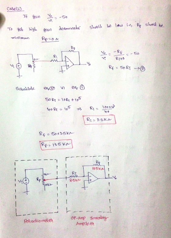
2, Design a variable gain amplifier using an inverting circuit and a 10 ΚΩ potentiometer. It...
P3. Using the circuit below to design the inverting amplifier having a gain of -10 and...
 P3. Using the circuit below to design the inverting amplifier having a gain of -10 and input resistance of 100 kΩ. Give the values of R1. 2 do
15. Design an inverting amplifier to have a gain of 20 using the MCP6021 and a...
15. Design an inverting amplifier to have a gain of 20 using the MCP6021 and a single +5 V supply. What will be the typical 3-dB bandwidth of the amplifier?
5.8 a) Design an inverting amplifier with a gain of 4. Use an ideal op amp,...
5.8 a) Design an inverting amplifier with a gain of 4. Use an ideal op amp, a resistor in the feedback path, and 12 V power supplies. b) Using your design from part (a), determine the range of input voltages that will keep the op amp in its linear operating region. c) Suppose you wish to amplify a 2 V signal, using your design from part (a) with a variable feedback resistor. What is the largest value of feedback resistance...
2. Design a non-inverting op-amp circuit with two resistors under the following conditions: a. The gain of the ampl...
 2. Design a non-inverting op-amp circuit with two resistors under the following conditions: a. The gain of the amplifier must be +10 b. The input range is ± 2V c. The total power consumed by the resistors must be less than 100 mW Show all the calculations required to design the amplifier circuit with the shown specifications.in details Use MULTISIM to create the op-amp circuit and print a fully labelled diagram of the circuits with the voltmeters displays showing both...
Design a difference amplifier circuit to yield a variable differential gain
Design a difference amplifier circuit to yield a variable differential gain in the range 1 to 100 and utilizing a 100 kΩ variable resistor. The design should include an ideal op-amp (Hint: Design the second stage for a gain of 0.5).
Assuming an ideal op-amp, design an inverting amplifier with a gain of 26 dB
Assuming an ideal op-amp, design an inverting amplifier with a gain of 26 dB having the largest possible R1 value under the constraint of having to use resistors no larger than 1 MΩ. If the input voltage source of this amplifier has an internal resistance r0 = 50 kΩ, how will this affect the gain? Design a solution that will eliminate the effect of the internal source resistance without having to change the values of R1 and R2.
please answer 3rd question using multisim 2-Design an inverting amplifier with a gain of -100 at...
 please answer 3rd question using multisim
2-Design an inverting amplifier with a gain of -100 at 100Hz. Increase the amplitude of the input signal until you observe clipping. Continue increasing the amplitude and observe the results. Briefly explain and comment your results 3-For the same amplifier as 2, increase the frequency of the input signal until you observe the slew rate characteristic associated with the Op Amp. Try different amplitudes Briefly explain and comment your results. 4- For the same...
please answer 3rd question using multisim
2-Design an inverting amplifier with a gain of -100 at 100Hz. Increase the amplitude of the input signal until you observe clipping. Continue increasing the amplitude and observe the results. Briefly explain and comment your results 3-For the same amplifier as 2, increase the frequency of the input signal until you observe the slew rate characteristic associated with the Op Amp. Try different amplitudes Briefly explain and comment your results. 4- For the same...
The circuit of Fig. 5.Sa is to be used as an inverting amplifier with a gain...
 The circuit of Fig. 5.Sa is to be used as an inverting amplifier with a gain of 10 VIV and is to employ the HA741C op amp. Specify suitable component values to ensure a maximum output error of 10 mV with minimum power dissipation in the resistors. Rt 0 FIGURE $.S
A. Design one circuit: Including power supply values and connections. 1-Design a non-inverting am...
A. Design one circuit: Including power supply values and connections. 1-Design a non-inverting amplifier with a gain of +11 V/V (+/- 10%) with an input of 0.5 V sin(2pi 200t). 2-Design an inverting amplifier with a gain of -22 V/V (+/- 10%) with an input of 0.12 V sin(2pi500t) 3-Design a 555 time astable with a 1 Hz output to an LED load 4-Design a single stage low-pass filter with a cutoff frequency of 300 Hz.
2. Construct the non-inverting amplifier circuit below. Then, obtain input-output transfer function for R1=1K and R2=2.2K,...
 2. Construct the non-inverting amplifier circuit below. Then, obtain input-output transfer function for R1=1K and R2=2.2K, E= 9V. Use a variable de voltage (5V de source and a variable 1k potentiometer) source as the input and measure the output voltage for different inputs. Draw the input-output transfer function from the measured input-output voltages. Proteus Table Vin Vout Measured Table Vin Vout Q2) Determine the voltage gain VO / Vin of the non-inverting amplifier. What is the output voltage range over...
 P3. Using the circuit below to design the inverting amplifier having a gain of -10 and input resistance of 100 kΩ. Give the values of R1. 2 do
 2. Design a non-inverting op-amp circuit with two resistors under the following conditions: a. The gain of the amplifier must be +10 b. The input range is ± 2V c. The total power consumed by the resistors must be less than 100 mW Show all the calculations required to design the amplifier circuit with the shown specifications.in details Use MULTISIM to create the op-amp circuit and print a fully labelled diagram of the circuits with the voltmeters displays showing both...
 please answer 3rd question using multisim
2-Design an inverting amplifier with a gain of -100 at 100Hz. Increase the amplitude of the input signal until you observe clipping. Continue increasing the amplitude and observe the results. Briefly explain and comment your results 3-For the same amplifier as 2, increase the frequency of the input signal until you observe the slew rate characteristic associated with the Op Amp. Try different amplitudes Briefly explain and comment your results. 4- For the same...
please answer 3rd question using multisim
2-Design an inverting amplifier with a gain of -100 at 100Hz. Increase the amplitude of the input signal until you observe clipping. Continue increasing the amplitude and observe the results. Briefly explain and comment your results 3-For the same amplifier as 2, increase the frequency of the input signal until you observe the slew rate characteristic associated with the Op Amp. Try different amplitudes Briefly explain and comment your results. 4- For the same...
 The circuit of Fig. 5.Sa is to be used as an inverting amplifier with a gain of 10 VIV and is to employ the HA741C op amp. Specify suitable component values to ensure a maximum output error of 10 mV with minimum power dissipation in the resistors. Rt 0 FIGURE $.S
 2. Construct the non-inverting amplifier circuit below. Then, obtain input-output transfer function for R1=1K and R2=2.2K, E= 9V. Use a variable de voltage (5V de source and a variable 1k potentiometer) source as the input and measure the output voltage for different inputs. Draw the input-output transfer function from the measured input-output voltages. Proteus Table Vin Vout Measured Table Vin Vout Q2) Determine the voltage gain VO / Vin of the non-inverting amplifier. What is the output voltage range over...
Most questions answered within 3 hours.
-
For this problem, carry at least four digits after the decimal
in your calculations. Answers may...
asked 1 hour ago -
Ask a user for three positive integer numbers. Use an input
validation loop to make sure...
asked 1 hour ago -
The most primitive form of data from data analysis perspective
is a. nominal scale b. ordinal...
asked 1 hour ago -
The number of vacancies in some hypothetical metal increases by
a factor of 5 when the...
asked 1 hour ago -
The fiduciary duty that is predicated on the concept that a
board of directors and officers...
asked 1 hour ago -
Sustainable Growth Rate Last year Umbrellas Unlimited
Corporation had an ROE of 17.3% and a dividend...
asked 1 hour ago -
Write a MATLAB program to do the following:
Receive 5 input values and store them into...
asked 1 hour ago -
Which one of the following aqueous solutions would you expect to
have the largest conductance: (a)...
asked 1 hour ago -
(Intermediate Macroeconomics)
2.The aggregate supply function be ys=2000+P, and the aggregate
demand function be yD=2400-P。Find the...
asked 1 hour ago -
I am having a really difficult time developing a strong thesis
for this question....... To what...
asked 2 hours ago -
There are n street lights in a line. In order to conserve
energy, the city decides...
asked 2 hours ago -
Cellular growth and repair require a cell to go through the cell
cycle. Like all biological...
asked 2 hours ago