

Homework Answers


Add Answer to:
may be use proposed circuit. what value should R have? solve
(i) and(iii). alpha,beta,gamma,epsilon=1
1. Design...
Do not mind the Greek Alph signs. Please explian steps and write clearly . Many Thanks!...
 Do not mind the Greek Alph signs. Please explian steps and
write clearly . Many Thanks!
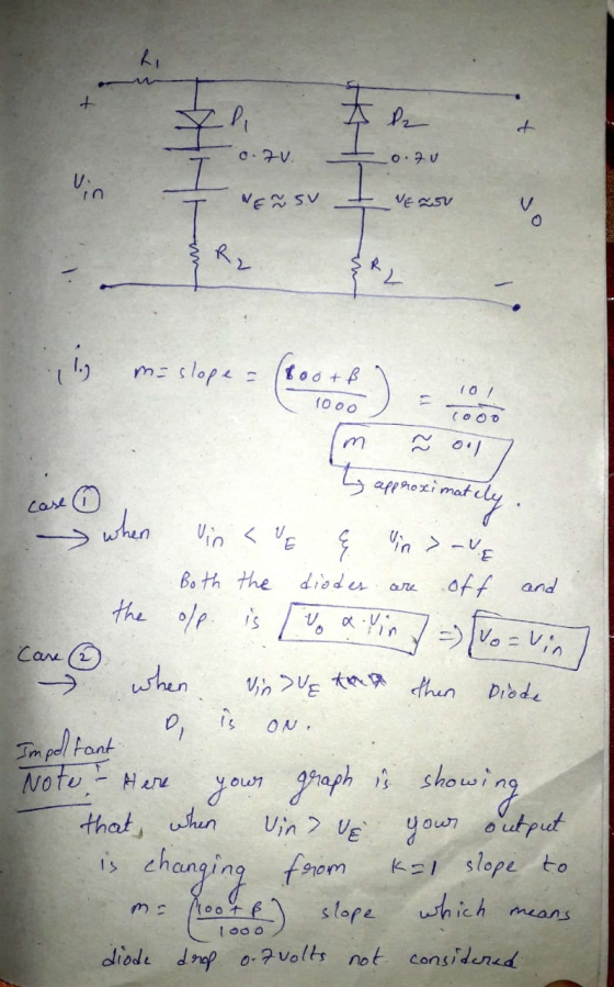
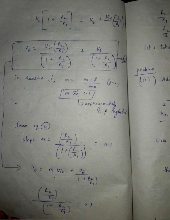
1. Design a circuit whose input-output characteristic is as shown in Figure 1. Slopem Slopek Ve Slope=m Figure 1 (0) Draw schematic and show the analysis that proves your design will operate as desired. You can assume that all diodes you use are ideal with a threshold of 0.7V. Take Ve = (5000+a) mV, m = (100+ By 1000 and k = 1. (4...
Do not mind the Greek Alph signs. Please explian steps and
write clearly . Many Thanks!
1. Design a circuit whose input-output characteristic is as shown in Figure 1. Slopem Slopek Ve Slope=m Figure 1 (0) Draw schematic and show the analysis that proves your design will operate as desired. You can assume that all diodes you use are ideal with a threshold of 0.7V. Take Ve = (5000+a) mV, m = (100+ By 1000 and k = 1. (4...
+10V Analysis Problems R voltage OV out 1) Design the given circuit configuration such that the...
 +10V Analysis Problems R voltage OV out 1) Design the given circuit configuration such that the output voltage -2.4V. Assume that the diodes available to you have a voltage drop of 0.7V across them when flowing a current of ImA. Also, the voltage across these diodes changes by 0.1V for every decade-change-in-the- current through them. Assume identical diodes. 1
please show steps, and solve asap BEE 433 Electronic Circuit Design Problem Set #1 Due date:...
 please show steps, and solve asap
BEE 433 Electronic Circuit Design Problem Set #1 Due date: Answer the following problems and Circle the answers. 1.1 (Fig. 1.1 from the textbook) In the voltage amplifier circuit of Fig. 1.1, let vs = 100 mV, Rs = 100 k 52, Vi = 75 mV, RL = 10 S2, and vo = 2 V. If connecting a 30-S2 resistance in parallel with RL drops vo to 1.8 V, find Ri, A., and R....
please show steps, and solve asap
BEE 433 Electronic Circuit Design Problem Set #1 Due date: Answer the following problems and Circle the answers. 1.1 (Fig. 1.1 from the textbook) In the voltage amplifier circuit of Fig. 1.1, let vs = 100 mV, Rs = 100 k 52, Vi = 75 mV, RL = 10 S2, and vo = 2 V. If connecting a 30-S2 resistance in parallel with RL drops vo to 1.8 V, find Ri, A., and R....
Problem 3: Design Problem On Figure P3a, you have a Common Source (CS) n-channel MOSFET amplifier....
 Problem 3: Design Problem On Figure P3a, you have a Common Source (CS) n-channel MOSFET amplifier. Notice the absence of a source resistor Rsig and load resistor R. If we know how the present amplifier (the one on Figure P3a) behaves without Rsig and RL, we can infer its behaviors if Rsig and R were to be added. design the amplifier circuit on Figure P3a, i.e., you have to find appropriate values for RGj You are to RG,, RD, and...
Procedure: 1. Assume that you have constructed the circuit from Figure 3. Since 57=5L/R is approximately...
 Procedure: 1. Assume that you have constructed the circuit from Figure 3. Since 57=5L/R is approximately 0.15 ms, steady-state conditions essentially exist as soon as the network is constructed, so you may do your analysis assuming steady state. 10v + >Ri= 1K2 V elem L= 10 mH V2 + M R2= 470 Figure 3 2. Calculate I, I1, and 12 assuming an ideal inductor (i.e. Rint= 0 2). Record the results in Table 2, first column. (2 points)
I want to solve this problem step by step 1. (35 points) Switch mode DC / DC Converters. a. (15 points) Design a flyback DC/DC power converter to the following specifications. Assume ideal compone...
 I want to solve this problem step by step
1. (35 points) Switch mode DC / DC Converters. a. (15 points) Design a flyback DC/DC power converter to the following specifications. Assume ideal components. Input Voltage Output Voltage Output Power Switching frequency Maximum Current Ripple in the filter inductor Output ripple voltage: Continuous conduction 170 VDC 12 VDC 40 Watts 750 kHz 1.2 Amps Your answer should include a circuit diagram with each energy storage element labeled with its value....
I want to solve this problem step by step
1. (35 points) Switch mode DC / DC Converters. a. (15 points) Design a flyback DC/DC power converter to the following specifications. Assume ideal components. Input Voltage Output Voltage Output Power Switching frequency Maximum Current Ripple in the filter inductor Output ripple voltage: Continuous conduction 170 VDC 12 VDC 40 Watts 750 kHz 1.2 Amps Your answer should include a circuit diagram with each energy storage element labeled with its value....
Can I get help with part g through part r, please? Given the following Common-Emitter Amplifier...
 Can I get help with part g through part r, please?
Given the following Common-Emitter Amplifier with Voltage-Divider Bias: The transistor is a Silicon device with B160 (Beta 160) and transistor r.= 30 kn: 20 V 34.7k LAL = Vou 35.10 31.1k LRE $3900 03 - Find the following quantities in parts a through where means Quiescent DC): a) Thevenin Voltage and Thevenin Resistance Re b) Base Current la Collector Current le d) Emitter Current le e) Transistor Collector-Emitter Quiescent...
Can I get help with part g through part r, please?
Given the following Common-Emitter Amplifier with Voltage-Divider Bias: The transistor is a Silicon device with B160 (Beta 160) and transistor r.= 30 kn: 20 V 34.7k LAL = Vou 35.10 31.1k LRE $3900 03 - Find the following quantities in parts a through where means Quiescent DC): a) Thevenin Voltage and Thevenin Resistance Re b) Base Current la Collector Current le d) Emitter Current le e) Transistor Collector-Emitter Quiescent...
Lab Preparation . Using DC analysis, and assuming that the transistors (QuEr and Q) are in...
 Lab Preparation . Using DC analysis, and assuming that the transistors (QuEr and Q) are in the active mode, determine the value of RREF required for generating a copy current of 0.755 mA. Take the value of Vcc to be 8 V, and the value of VE in the active mode to be equal to 0.7V. Vee H Qur о RaI Figure 3 Single-stage amplifier biased by a simple current miror device 2. The circuit shown in Figure 3, is...
Yes, this is one problem. Please solve ALL PARTS. Guaranteed thumbs up for the person who solves it. 3 1. Photodiode...
 Yes, this is one problem. Please solve ALL PARTS. Guaranteed
thumbs up for the person who solves it.
3 1. Photodiode amplifier circuit You are designinga CF photosensor circuit for a light detection and ranging LiDAR) system in autonomous vehicles. The circuit utilizes a transimpedance amplifier to convert low-level RF photodiode current signal to a usable voltage output. It consists of a photodiode, an amplifier, and feedback capacitor/resistor pair as shown in Figure 1. We will derive simple equations to...
Yes, this is one problem. Please solve ALL PARTS. Guaranteed
thumbs up for the person who solves it.
3 1. Photodiode amplifier circuit You are designinga CF photosensor circuit for a light detection and ranging LiDAR) system in autonomous vehicles. The circuit utilizes a transimpedance amplifier to convert low-level RF photodiode current signal to a usable voltage output. It consists of a photodiode, an amplifier, and feedback capacitor/resistor pair as shown in Figure 1. We will derive simple equations to...
I am currently trying to figure out the experiment below. Please complete Table 1 with an...
 I am currently trying to figure out the experiment below. Please
complete Table 1 with an explanation, I appreciate it thank
you! Promise to give thumbs up!
Introduction The phase differences between the output voltage, the voltage across the inductor, the voltage across the capacitor, and the voltage across the resistor will be examined at resonant frequency. The voltage and phase relationship will also be examined for frequencies above and below resonance. Theory An inductor, a capacitor, and a resistor are...
I am currently trying to figure out the experiment below. Please
complete Table 1 with an explanation, I appreciate it thank
you! Promise to give thumbs up!
Introduction The phase differences between the output voltage, the voltage across the inductor, the voltage across the capacitor, and the voltage across the resistor will be examined at resonant frequency. The voltage and phase relationship will also be examined for frequencies above and below resonance. Theory An inductor, a capacitor, and a resistor are...
 Do not mind the Greek Alph signs. Please explian steps and
write clearly . Many Thanks!
1. Design a circuit whose input-output characteristic is as shown in Figure 1. Slopem Slopek Ve Slope=m Figure 1 (0) Draw schematic and show the analysis that proves your design will operate as desired. You can assume that all diodes you use are ideal with a threshold of 0.7V. Take Ve = (5000+a) mV, m = (100+ By 1000 and k = 1. (4...
Do not mind the Greek Alph signs. Please explian steps and
write clearly . Many Thanks!
1. Design a circuit whose input-output characteristic is as shown in Figure 1. Slopem Slopek Ve Slope=m Figure 1 (0) Draw schematic and show the analysis that proves your design will operate as desired. You can assume that all diodes you use are ideal with a threshold of 0.7V. Take Ve = (5000+a) mV, m = (100+ By 1000 and k = 1. (4...
 +10V Analysis Problems R voltage OV out 1) Design the given circuit configuration such that the output voltage -2.4V. Assume that the diodes available to you have a voltage drop of 0.7V across them when flowing a current of ImA. Also, the voltage across these diodes changes by 0.1V for every decade-change-in-the- current through them. Assume identical diodes. 1
 please show steps, and solve asap
BEE 433 Electronic Circuit Design Problem Set #1 Due date: Answer the following problems and Circle the answers. 1.1 (Fig. 1.1 from the textbook) In the voltage amplifier circuit of Fig. 1.1, let vs = 100 mV, Rs = 100 k 52, Vi = 75 mV, RL = 10 S2, and vo = 2 V. If connecting a 30-S2 resistance in parallel with RL drops vo to 1.8 V, find Ri, A., and R....
please show steps, and solve asap
BEE 433 Electronic Circuit Design Problem Set #1 Due date: Answer the following problems and Circle the answers. 1.1 (Fig. 1.1 from the textbook) In the voltage amplifier circuit of Fig. 1.1, let vs = 100 mV, Rs = 100 k 52, Vi = 75 mV, RL = 10 S2, and vo = 2 V. If connecting a 30-S2 resistance in parallel with RL drops vo to 1.8 V, find Ri, A., and R....
 Problem 3: Design Problem On Figure P3a, you have a Common Source (CS) n-channel MOSFET amplifier. Notice the absence of a source resistor Rsig and load resistor R. If we know how the present amplifier (the one on Figure P3a) behaves without Rsig and RL, we can infer its behaviors if Rsig and R were to be added. design the amplifier circuit on Figure P3a, i.e., you have to find appropriate values for RGj You are to RG,, RD, and...
 Procedure: 1. Assume that you have constructed the circuit from Figure 3. Since 57=5L/R is approximately 0.15 ms, steady-state conditions essentially exist as soon as the network is constructed, so you may do your analysis assuming steady state. 10v + >Ri= 1K2 V elem L= 10 mH V2 + M R2= 470 Figure 3 2. Calculate I, I1, and 12 assuming an ideal inductor (i.e. Rint= 0 2). Record the results in Table 2, first column. (2 points)
 I want to solve this problem step by step
1. (35 points) Switch mode DC / DC Converters. a. (15 points) Design a flyback DC/DC power converter to the following specifications. Assume ideal components. Input Voltage Output Voltage Output Power Switching frequency Maximum Current Ripple in the filter inductor Output ripple voltage: Continuous conduction 170 VDC 12 VDC 40 Watts 750 kHz 1.2 Amps Your answer should include a circuit diagram with each energy storage element labeled with its value....
I want to solve this problem step by step
1. (35 points) Switch mode DC / DC Converters. a. (15 points) Design a flyback DC/DC power converter to the following specifications. Assume ideal components. Input Voltage Output Voltage Output Power Switching frequency Maximum Current Ripple in the filter inductor Output ripple voltage: Continuous conduction 170 VDC 12 VDC 40 Watts 750 kHz 1.2 Amps Your answer should include a circuit diagram with each energy storage element labeled with its value....
 Can I get help with part g through part r, please?
Given the following Common-Emitter Amplifier with Voltage-Divider Bias: The transistor is a Silicon device with B160 (Beta 160) and transistor r.= 30 kn: 20 V 34.7k LAL = Vou 35.10 31.1k LRE $3900 03 - Find the following quantities in parts a through where means Quiescent DC): a) Thevenin Voltage and Thevenin Resistance Re b) Base Current la Collector Current le d) Emitter Current le e) Transistor Collector-Emitter Quiescent...
Can I get help with part g through part r, please?
Given the following Common-Emitter Amplifier with Voltage-Divider Bias: The transistor is a Silicon device with B160 (Beta 160) and transistor r.= 30 kn: 20 V 34.7k LAL = Vou 35.10 31.1k LRE $3900 03 - Find the following quantities in parts a through where means Quiescent DC): a) Thevenin Voltage and Thevenin Resistance Re b) Base Current la Collector Current le d) Emitter Current le e) Transistor Collector-Emitter Quiescent...
 Lab Preparation . Using DC analysis, and assuming that the transistors (QuEr and Q) are in the active mode, determine the value of RREF required for generating a copy current of 0.755 mA. Take the value of Vcc to be 8 V, and the value of VE in the active mode to be equal to 0.7V. Vee H Qur о RaI Figure 3 Single-stage amplifier biased by a simple current miror device 2. The circuit shown in Figure 3, is...
 Yes, this is one problem. Please solve ALL PARTS. Guaranteed
thumbs up for the person who solves it.
3 1. Photodiode amplifier circuit You are designinga CF photosensor circuit for a light detection and ranging LiDAR) system in autonomous vehicles. The circuit utilizes a transimpedance amplifier to convert low-level RF photodiode current signal to a usable voltage output. It consists of a photodiode, an amplifier, and feedback capacitor/resistor pair as shown in Figure 1. We will derive simple equations to...
Yes, this is one problem. Please solve ALL PARTS. Guaranteed
thumbs up for the person who solves it.
3 1. Photodiode amplifier circuit You are designinga CF photosensor circuit for a light detection and ranging LiDAR) system in autonomous vehicles. The circuit utilizes a transimpedance amplifier to convert low-level RF photodiode current signal to a usable voltage output. It consists of a photodiode, an amplifier, and feedback capacitor/resistor pair as shown in Figure 1. We will derive simple equations to...
 I am currently trying to figure out the experiment below. Please
complete Table 1 with an explanation, I appreciate it thank
you! Promise to give thumbs up!
Introduction The phase differences between the output voltage, the voltage across the inductor, the voltage across the capacitor, and the voltage across the resistor will be examined at resonant frequency. The voltage and phase relationship will also be examined for frequencies above and below resonance. Theory An inductor, a capacitor, and a resistor are...
I am currently trying to figure out the experiment below. Please
complete Table 1 with an explanation, I appreciate it thank
you! Promise to give thumbs up!
Introduction The phase differences between the output voltage, the voltage across the inductor, the voltage across the capacitor, and the voltage across the resistor will be examined at resonant frequency. The voltage and phase relationship will also be examined for frequencies above and below resonance. Theory An inductor, a capacitor, and a resistor are...
Most questions answered within 3 hours.
-
Write a program to solve the Josephus problem, with the following
modification:
Sample Input:
./a.out n...
asked 2 hours ago -
At the start of a CD it is spinning at a rate of 525 rpm
(revolutions...
asked 2 hours ago -
4. Without doing any calculations, predict whether the observed
∆T would increase, decrease or remain the...
asked 3 hours ago -
Based on the range, which of the following sets of scores has
the greatest variability? 3,...
asked 5 hours ago -
Ripples in a pond travel at a velocity of 3 m/s with one peak
passing a...
asked 4 hours ago -
A man stands on the roof of a building of height 13.0 mm and
throws a...
asked 4 hours ago -
The extent to which assets are financed by borrowed funds and
other liabilities is indicated by:...
asked 6 hours ago -
Explain in detail
Germany is the fifth largest economy
explain what goods and services Germany specializes...
asked 6 hours ago -
The density of platinum is 21.45 g/mL. If a cube of platinum
with a mass of...
asked 6 hours ago -
Accounts Receivable
Sales
A/R Posting
Extended Sales Invoice
Packing Slip
Compare invoice to packing slip 2...
asked 6 hours ago -
Michaella, age 23, is a full-time law student and is claimed by
her parents as a...
asked 6 hours ago -
Why are polymers not typically casted into products?
asked 6 hours ago