
Homework Answers


Add Answer to:
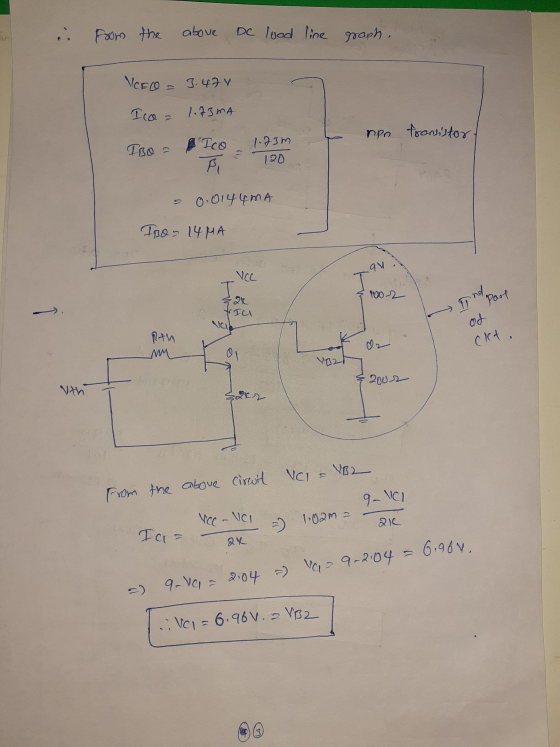
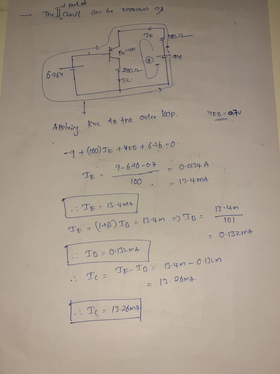
2. (20%). In the circult shown below, the DC current gain for the npn translator is...
Shown below is a single stage common emitter amplifier with a unipolar dc power supply using an 2...
 Shown below is a single stage common emitter amplifier with a unipolar dc power supply using an 2N3904 NPN BJT as the active device. It is specified that V+ 40 V, C1 C2CE 100uF, Ro-7.5 k2, REi-5.1kS2, and Ri - 36k52. Design the circuit so that the dc collector current is 2 mA and the magnitude of the small-signal midband voltage gain is 32.3. For the design calculations assume that the base-to- emitter dc voltage drop is 0.65 V, the...
An analogue amplifier circuit is shown in Figure 1 below. VDD Q5 15V JL - Vout...
 An analogue amplifier circuit is shown in Figure 1 below. VDD Q5 15V JL - Vout Irer RI Vina JET T7T Figure 1 Integrated amplifier circuit. Circuit Data: Vpp = 15 V, IREF = I1 = I2 = 1.0 mA Transistor Data: Q1: NMOS, un Cox = 80 A/V?, W/L = 100 um/0.8 um, Vtn = 0.8 V, L = 0.10 um/V Q2: NPN BJT, B = 100, Vbe = 0.7 V, VA = 150 V Q3, Q4: NMOS, un...
Laboratory 2: Transistor circuit characteristics A. Objectives: 1. To study the basic characteris...
 Laboratory 2: Transistor circuit characteristics A. Objectives: 1. To study the basic characteristics of a transistor circuit. 2. To study the bias circuit of a transistor circuit. B. Apparatus: 1. DC Power supply 2. Experimental boards and corresponding components 3. Electronic calculator (prepared by students) 4. Digital camera (prepared by students for photo taking of the experimental results) 5. Laptop computer with the software PicoScope 6 and Microsoft Word installed. 6. PicoScope PC Oscilloscope and its accessories. 7. Digital multi-meter....
 Shown below is a single stage common emitter amplifier with a unipolar dc power supply using an 2N3904 NPN BJT as the active device. It is specified that V+ 40 V, C1 C2CE 100uF, Ro-7.5 k2, REi-5.1kS2, and Ri - 36k52. Design the circuit so that the dc collector current is 2 mA and the magnitude of the small-signal midband voltage gain is 32.3. For the design calculations assume that the base-to- emitter dc voltage drop is 0.65 V, the...
 An analogue amplifier circuit is shown in Figure 1 below. VDD Q5 15V JL - Vout Irer RI Vina JET T7T Figure 1 Integrated amplifier circuit. Circuit Data: Vpp = 15 V, IREF = I1 = I2 = 1.0 mA Transistor Data: Q1: NMOS, un Cox = 80 A/V?, W/L = 100 um/0.8 um, Vtn = 0.8 V, L = 0.10 um/V Q2: NPN BJT, B = 100, Vbe = 0.7 V, VA = 150 V Q3, Q4: NMOS, un...
 Laboratory 2: Transistor circuit characteristics A. Objectives: 1. To study the basic characteristics of a transistor circuit. 2. To study the bias circuit of a transistor circuit. B. Apparatus: 1. DC Power supply 2. Experimental boards and corresponding components 3. Electronic calculator (prepared by students) 4. Digital camera (prepared by students for photo taking of the experimental results) 5. Laptop computer with the software PicoScope 6 and Microsoft Word installed. 6. PicoScope PC Oscilloscope and its accessories. 7. Digital multi-meter....
Most questions answered within 3 hours.
-
Montecino Corporation uses two different types of labor to
manufacture its product. The types of labor,...
asked 9 minutes ago -
4. What are the two possible products of the
intramolecular hemiacetal formation of linear glucose?
5. ...
asked 30 minutes ago -
The opportunity cost of attending university is likely to
include all except which of the following?...
asked 33 minutes ago -
Consider the following regular
expression: (a*bc+d*e)*
Transform this regular expression to an NFA, from
there to...
asked 29 minutes ago -
1. The Janjua Company had the following account balances at
1/1/16: Common Stock $50,000 Treasury Stock...
asked 30 minutes ago -
A solution with maximum solute that can dissolve and remain
stable is
saturated
unsaturated
miscible
supersaturated
asked 35 minutes ago -
Describe how you would make 100ml of a 10mmol glucose
standard
asked 35 minutes ago -
Zahn Corp.'s comparative balance sheet at December 31, 20x5 and
20x4, reported accumulated depreciation balances of...
asked 36 minutes ago -
How many milliliters of 5.6 M NaOH are needed to neutralize 3.9
mL of a 6.6...
asked 47 minutes ago -
Will dislike
if you don't code efficiently, you must have knowledge of
next.js,vue.js,immutable.js,react,js.
Develop an api...
asked 53 minutes ago -
When financial statements are converted to percentages, they are
referred to as:
A. Percent of change...
asked 54 minutes ago -
16) Which of the following is not a way to reduce the
government's budget
deficit
A)...
asked 1 hour ago