
2 6
Homework Answers


Add Answer to:
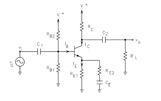
Shown below is a single stage common emitter amplifier with a unipolar dc power supply using an 2...
FIND THE VALUES OF Rb1, Rb2, Re,Rc, rin , rout, overall gain and open circuit gain First, design a common emitter BJT a...
 FIND THE VALUES OF Rb1, Rb2, Re,Rc, rin , rout, overall gain and
open circuit gain
First, design a common emitter BJT amplifier Second, analyze the amplifier.( Avo, Gv, Rin, Rout) Third, compare your calculation with Multisim. Report must include comparison between your calculation & simulation results overall voltage gain, open circuit voltage gain, input resistance, and output resistance. This design project is not group work, must be done individually. Type your report. Design a discrete common emitter BJT amplifier.(Determine...
FIND THE VALUES OF Rb1, Rb2, Re,Rc, rin , rout, overall gain and
open circuit gain
First, design a common emitter BJT amplifier Second, analyze the amplifier.( Avo, Gv, Rin, Rout) Third, compare your calculation with Multisim. Report must include comparison between your calculation & simulation results overall voltage gain, open circuit voltage gain, input resistance, and output resistance. This design project is not group work, must be done individually. Type your report. Design a discrete common emitter BJT amplifier.(Determine...
(10 pts) Consider a common-emitter amplifier with emitter resistor shown below. DC voltage source...
 Common-emitter amplifier?
(10 pts) Consider a common-emitter amplifier with emitter resistor shown below. DC voltage sources VBB and Vcc bias the transistor at lc-1mA. Let β-100. Determine the overall voltage gain Gv 2. VCC 10 k2 Vsig VBB
(10 pts) Consider a common-emitter amplifier with emitter resistor shown below. DC voltage sources VBB and Vcc bias the transistor at lc-1mA. Let β-100. Determine the overall voltage gain Gv 2. VCC 10 k2 Vsig VBB
Common-emitter amplifier?
(10 pts) Consider a common-emitter amplifier with emitter resistor shown below. DC voltage sources VBB and Vcc bias the transistor at lc-1mA. Let β-100. Determine the overall voltage gain Gv 2. VCC 10 k2 Vsig VBB
(10 pts) Consider a common-emitter amplifier with emitter resistor shown below. DC voltage sources VBB and Vcc bias the transistor at lc-1mA. Let β-100. Determine the overall voltage gain Gv 2. VCC 10 k2 Vsig VBB
Vsig = 10mV*sin(2Kπ) The circuit above is a common-emitter amplifier. Given the parameters in the circuit,...
 Vsig = 10mV*sin(2Kπ)
The circuit above is a common-emitter amplifier. Given the
parameters in the circuit,
1. If Rb1=10KΩ, Calculate Rb2, Ib, Ic, Ie, Re, transconductance
(gm), Current through Rb1 (I_rb1), and Current through Rb2(I_rb2),
Vb, Vc, Ve, Vce. Also, calculate Rc to achieve a voltage gain Av =
- 100 V/
(If Rb1 value does not match up, then choose your resistor
value for Rb1.)
2. If the amplitude of Vsig keeps increasing, at what amplitude
of the input...
Vsig = 10mV*sin(2Kπ)
The circuit above is a common-emitter amplifier. Given the
parameters in the circuit,
1. If Rb1=10KΩ, Calculate Rb2, Ib, Ic, Ie, Re, transconductance
(gm), Current through Rb1 (I_rb1), and Current through Rb2(I_rb2),
Vb, Vc, Ve, Vce. Also, calculate Rc to achieve a voltage gain Av =
- 100 V/
(If Rb1 value does not match up, then choose your resistor
value for Rb1.)
2. If the amplitude of Vsig keeps increasing, at what amplitude
of the input...
Perform a simple initial design of an ac coupled common-emitter amplifier with four resistor biasing and emitter by-pass...
 Perform a simple initial design of an ac coupled common-emitter
amplifier with
four resistor biasing and emitter by-pass capacitor, to have a
voltage gain of about
100, for the following conditions. Justify any approximations used.
(Assume Ic=1/300 A)
i)Transistor ac common-emitter gain, B, 100 ii) Supply voltage ofV0c-20V iii) Allow 10% Vcc across RE DC collector voltage of 10 V iv) v) DC current in the base bias resistors should be ten times greater than the DC base current. Assume...
Perform a simple initial design of an ac coupled common-emitter
amplifier with
four resistor biasing and emitter by-pass capacitor, to have a
voltage gain of about
100, for the following conditions. Justify any approximations used.
(Assume Ic=1/300 A)
i)Transistor ac common-emitter gain, B, 100 ii) Supply voltage ofV0c-20V iii) Allow 10% Vcc across RE DC collector voltage of 10 V iv) v) DC current in the base bias resistors should be ten times greater than the DC base current. Assume...
1. Design the common-emitter amplifier in Fig. 4(a) with the following specifications: Supply Vol...
 Figure 4. (a)
1. Design the common-emitter amplifier in Fig. 4(a) with the following specifications: Supply Voltage, Vcc 0-to-Peak Output Swing, V Voltage Gain, A. Input Resistance, R Output Resistance, Ro THD for 5kHz 1 V (0-to-peak) Sine Wave Output Voltage, V Relative Variation of Ic for VBE 0.7t 0.1V Transistor's Current Gain, β 5V 25 1.8kS2 4% 10% 100 Show your design procedure and all your calculations. Your design should be insensitive to B variations. Vcc RB1 Rc 0...
Figure 4. (a)
1. Design the common-emitter amplifier in Fig. 4(a) with the following specifications: Supply Voltage, Vcc 0-to-Peak Output Swing, V Voltage Gain, A. Input Resistance, R Output Resistance, Ro THD for 5kHz 1 V (0-to-peak) Sine Wave Output Voltage, V Relative Variation of Ic for VBE 0.7t 0.1V Transistor's Current Gain, β 5V 25 1.8kS2 4% 10% 100 Show your design procedure and all your calculations. Your design should be insensitive to B variations. Vcc RB1 Rc 0...
Design a BJT amplifier based on the specifications provided in the table below. Your design shoul...
 THE STEPS TO DO SO:
Design a BJT amplifier based on the specifications provided in the table below. Your design should be insensitive to β variations, and both the input and the output should be AC coupled as in Fig. 1. Supply Voltage, Vcc Load Resistance, RL Transistor's Current Gain, β Relative Variation of lc for VBE-0.7 ± 0.1 V 0-to-Peak Output Swing, Vo Voltage Gain, A Input Resistance, R THD for 5kHz IV (0-to-peak) Sine Wave Output Voltage, V。S5%...
THE STEPS TO DO SO:
Design a BJT amplifier based on the specifications provided in the table below. Your design should be insensitive to β variations, and both the input and the output should be AC coupled as in Fig. 1. Supply Voltage, Vcc Load Resistance, RL Transistor's Current Gain, β Relative Variation of lc for VBE-0.7 ± 0.1 V 0-to-Peak Output Swing, Vo Voltage Gain, A Input Resistance, R THD for 5kHz IV (0-to-peak) Sine Wave Output Voltage, V。S5%...
Can I get help with part g through part r, please? Given the following Common-Emitter Amplifier...
 Can I get help with part g through part r, please?
Given the following Common-Emitter Amplifier with Voltage-Divider Bias: The transistor is a Silicon device with B160 (Beta 160) and transistor r.= 30 kn: 20 V 34.7k LAL = Vou 35.10 31.1k LRE $3900 03 - Find the following quantities in parts a through where means Quiescent DC): a) Thevenin Voltage and Thevenin Resistance Re b) Base Current la Collector Current le d) Emitter Current le e) Transistor Collector-Emitter Quiescent...
Can I get help with part g through part r, please?
Given the following Common-Emitter Amplifier with Voltage-Divider Bias: The transistor is a Silicon device with B160 (Beta 160) and transistor r.= 30 kn: 20 V 34.7k LAL = Vou 35.10 31.1k LRE $3900 03 - Find the following quantities in parts a through where means Quiescent DC): a) Thevenin Voltage and Thevenin Resistance Re b) Base Current la Collector Current le d) Emitter Current le e) Transistor Collector-Emitter Quiescent...
4. The amplifier shown below has Rsig-RL 1kQ. Rc 1kQ, RB 47 kQ. β 100, Cc1 a) Find the dc collect...
 4. The amplifier shown below has Rsig-RL 1kQ. Rc 1kQ, RB 47 kQ. β 100, Cc1 a) Find the dc collector current of the transistor b) Find gm and IT c) Neglecting ro, find the midband voltage gain from base to collector (neglect the effect of RB) d) Use the gain obtained in part (c) to find the component of Rin that arises as a result of RB. Hence find Rin. e) Find the overall gain at midband f) Find...
You are required to design a 2-stage voltage amplifier (find values for RE, RC1, RC2) to meet the following criteria: an...
 You are required to design a 2-stage voltage amplifier (find
values for RE, RC1, RC2) to meet the following criteria: an input
resistance of 400 kΩ and an overall voltage gain equal to or
greater than 250, with a resistor output load, RL. Use a
common-emitter with emitter degradation (RE) stage for the input,
followed by a commonemitter amplifier with bias current equal to
0.5 mA. (VCC = 20 V, βo = 200 and the DC levels of the first...
You are required to design a 2-stage voltage amplifier (find
values for RE, RC1, RC2) to meet the following criteria: an input
resistance of 400 kΩ and an overall voltage gain equal to or
greater than 250, with a resistor output load, RL. Use a
common-emitter with emitter degradation (RE) stage for the input,
followed by a commonemitter amplifier with bias current equal to
0.5 mA. (VCC = 20 V, βo = 200 and the DC levels of the first...
please I need details l and....Debate Club | Offic A) Theoretical Design Design a common emitter BJT amplifier with the following requirements: -Rin-10 K2, and Ro-45 ㏀ (Neglect the Early voltage...
 please I need details
l and....Debate Club | Offic A) Theoretical Design Design a common emitter BJT amplifier with the following requirements: -Rin-10 K2, and Ro-45 ㏀ (Neglect the Early voltage Effect) Vo/Vsig- Gv-40 VIV or 32 dB " VCC-9 V V, IC-1mA, VCE-3.25V and β-100 RL-40 kQ, Rsige I ka, R 1-3R2, and C1-C2-1 μF Voc RC C2 R1 Rsig C1 RL R2 RE B) Verify your design using Orcad Capture Pspice by doing 1) AC sweep (frequency response):...
please I need details
l and....Debate Club | Offic A) Theoretical Design Design a common emitter BJT amplifier with the following requirements: -Rin-10 K2, and Ro-45 ㏀ (Neglect the Early voltage Effect) Vo/Vsig- Gv-40 VIV or 32 dB " VCC-9 V V, IC-1mA, VCE-3.25V and β-100 RL-40 kQ, Rsige I ka, R 1-3R2, and C1-C2-1 μF Voc RC C2 R1 Rsig C1 RL R2 RE B) Verify your design using Orcad Capture Pspice by doing 1) AC sweep (frequency response):...
 FIND THE VALUES OF Rb1, Rb2, Re,Rc, rin , rout, overall gain and
open circuit gain
First, design a common emitter BJT amplifier Second, analyze the amplifier.( Avo, Gv, Rin, Rout) Third, compare your calculation with Multisim. Report must include comparison between your calculation & simulation results overall voltage gain, open circuit voltage gain, input resistance, and output resistance. This design project is not group work, must be done individually. Type your report. Design a discrete common emitter BJT amplifier.(Determine...
FIND THE VALUES OF Rb1, Rb2, Re,Rc, rin , rout, overall gain and
open circuit gain
First, design a common emitter BJT amplifier Second, analyze the amplifier.( Avo, Gv, Rin, Rout) Third, compare your calculation with Multisim. Report must include comparison between your calculation & simulation results overall voltage gain, open circuit voltage gain, input resistance, and output resistance. This design project is not group work, must be done individually. Type your report. Design a discrete common emitter BJT amplifier.(Determine...
 Common-emitter amplifier?
(10 pts) Consider a common-emitter amplifier with emitter resistor shown below. DC voltage sources VBB and Vcc bias the transistor at lc-1mA. Let β-100. Determine the overall voltage gain Gv 2. VCC 10 k2 Vsig VBB
(10 pts) Consider a common-emitter amplifier with emitter resistor shown below. DC voltage sources VBB and Vcc bias the transistor at lc-1mA. Let β-100. Determine the overall voltage gain Gv 2. VCC 10 k2 Vsig VBB
Common-emitter amplifier?
(10 pts) Consider a common-emitter amplifier with emitter resistor shown below. DC voltage sources VBB and Vcc bias the transistor at lc-1mA. Let β-100. Determine the overall voltage gain Gv 2. VCC 10 k2 Vsig VBB
(10 pts) Consider a common-emitter amplifier with emitter resistor shown below. DC voltage sources VBB and Vcc bias the transistor at lc-1mA. Let β-100. Determine the overall voltage gain Gv 2. VCC 10 k2 Vsig VBB
 Vsig = 10mV*sin(2Kπ)
The circuit above is a common-emitter amplifier. Given the
parameters in the circuit,
1. If Rb1=10KΩ, Calculate Rb2, Ib, Ic, Ie, Re, transconductance
(gm), Current through Rb1 (I_rb1), and Current through Rb2(I_rb2),
Vb, Vc, Ve, Vce. Also, calculate Rc to achieve a voltage gain Av =
- 100 V/
(If Rb1 value does not match up, then choose your resistor
value for Rb1.)
2. If the amplitude of Vsig keeps increasing, at what amplitude
of the input...
Vsig = 10mV*sin(2Kπ)
The circuit above is a common-emitter amplifier. Given the
parameters in the circuit,
1. If Rb1=10KΩ, Calculate Rb2, Ib, Ic, Ie, Re, transconductance
(gm), Current through Rb1 (I_rb1), and Current through Rb2(I_rb2),
Vb, Vc, Ve, Vce. Also, calculate Rc to achieve a voltage gain Av =
- 100 V/
(If Rb1 value does not match up, then choose your resistor
value for Rb1.)
2. If the amplitude of Vsig keeps increasing, at what amplitude
of the input...
 Perform a simple initial design of an ac coupled common-emitter
amplifier with
four resistor biasing and emitter by-pass capacitor, to have a
voltage gain of about
100, for the following conditions. Justify any approximations used.
(Assume Ic=1/300 A)
i)Transistor ac common-emitter gain, B, 100 ii) Supply voltage ofV0c-20V iii) Allow 10% Vcc across RE DC collector voltage of 10 V iv) v) DC current in the base bias resistors should be ten times greater than the DC base current. Assume...
Perform a simple initial design of an ac coupled common-emitter
amplifier with
four resistor biasing and emitter by-pass capacitor, to have a
voltage gain of about
100, for the following conditions. Justify any approximations used.
(Assume Ic=1/300 A)
i)Transistor ac common-emitter gain, B, 100 ii) Supply voltage ofV0c-20V iii) Allow 10% Vcc across RE DC collector voltage of 10 V iv) v) DC current in the base bias resistors should be ten times greater than the DC base current. Assume...
 Figure 4. (a)
1. Design the common-emitter amplifier in Fig. 4(a) with the following specifications: Supply Voltage, Vcc 0-to-Peak Output Swing, V Voltage Gain, A. Input Resistance, R Output Resistance, Ro THD for 5kHz 1 V (0-to-peak) Sine Wave Output Voltage, V Relative Variation of Ic for VBE 0.7t 0.1V Transistor's Current Gain, β 5V 25 1.8kS2 4% 10% 100 Show your design procedure and all your calculations. Your design should be insensitive to B variations. Vcc RB1 Rc 0...
Figure 4. (a)
1. Design the common-emitter amplifier in Fig. 4(a) with the following specifications: Supply Voltage, Vcc 0-to-Peak Output Swing, V Voltage Gain, A. Input Resistance, R Output Resistance, Ro THD for 5kHz 1 V (0-to-peak) Sine Wave Output Voltage, V Relative Variation of Ic for VBE 0.7t 0.1V Transistor's Current Gain, β 5V 25 1.8kS2 4% 10% 100 Show your design procedure and all your calculations. Your design should be insensitive to B variations. Vcc RB1 Rc 0...
 THE STEPS TO DO SO:
Design a BJT amplifier based on the specifications provided in the table below. Your design should be insensitive to β variations, and both the input and the output should be AC coupled as in Fig. 1. Supply Voltage, Vcc Load Resistance, RL Transistor's Current Gain, β Relative Variation of lc for VBE-0.7 ± 0.1 V 0-to-Peak Output Swing, Vo Voltage Gain, A Input Resistance, R THD for 5kHz IV (0-to-peak) Sine Wave Output Voltage, V。S5%...
THE STEPS TO DO SO:
Design a BJT amplifier based on the specifications provided in the table below. Your design should be insensitive to β variations, and both the input and the output should be AC coupled as in Fig. 1. Supply Voltage, Vcc Load Resistance, RL Transistor's Current Gain, β Relative Variation of lc for VBE-0.7 ± 0.1 V 0-to-Peak Output Swing, Vo Voltage Gain, A Input Resistance, R THD for 5kHz IV (0-to-peak) Sine Wave Output Voltage, V。S5%...
 Can I get help with part g through part r, please?
Given the following Common-Emitter Amplifier with Voltage-Divider Bias: The transistor is a Silicon device with B160 (Beta 160) and transistor r.= 30 kn: 20 V 34.7k LAL = Vou 35.10 31.1k LRE $3900 03 - Find the following quantities in parts a through where means Quiescent DC): a) Thevenin Voltage and Thevenin Resistance Re b) Base Current la Collector Current le d) Emitter Current le e) Transistor Collector-Emitter Quiescent...
Can I get help with part g through part r, please?
Given the following Common-Emitter Amplifier with Voltage-Divider Bias: The transistor is a Silicon device with B160 (Beta 160) and transistor r.= 30 kn: 20 V 34.7k LAL = Vou 35.10 31.1k LRE $3900 03 - Find the following quantities in parts a through where means Quiescent DC): a) Thevenin Voltage and Thevenin Resistance Re b) Base Current la Collector Current le d) Emitter Current le e) Transistor Collector-Emitter Quiescent...
 4. The amplifier shown below has Rsig-RL 1kQ. Rc 1kQ, RB 47 kQ. β 100, Cc1 a) Find the dc collector current of the transistor b) Find gm and IT c) Neglecting ro, find the midband voltage gain from base to collector (neglect the effect of RB) d) Use the gain obtained in part (c) to find the component of Rin that arises as a result of RB. Hence find Rin. e) Find the overall gain at midband f) Find...
 You are required to design a 2-stage voltage amplifier (find
values for RE, RC1, RC2) to meet the following criteria: an input
resistance of 400 kΩ and an overall voltage gain equal to or
greater than 250, with a resistor output load, RL. Use a
common-emitter with emitter degradation (RE) stage for the input,
followed by a commonemitter amplifier with bias current equal to
0.5 mA. (VCC = 20 V, βo = 200 and the DC levels of the first...
You are required to design a 2-stage voltage amplifier (find
values for RE, RC1, RC2) to meet the following criteria: an input
resistance of 400 kΩ and an overall voltage gain equal to or
greater than 250, with a resistor output load, RL. Use a
common-emitter with emitter degradation (RE) stage for the input,
followed by a commonemitter amplifier with bias current equal to
0.5 mA. (VCC = 20 V, βo = 200 and the DC levels of the first...
 please I need details
l and....Debate Club | Offic A) Theoretical Design Design a common emitter BJT amplifier with the following requirements: -Rin-10 K2, and Ro-45 ㏀ (Neglect the Early voltage Effect) Vo/Vsig- Gv-40 VIV or 32 dB " VCC-9 V V, IC-1mA, VCE-3.25V and β-100 RL-40 kQ, Rsige I ka, R 1-3R2, and C1-C2-1 μF Voc RC C2 R1 Rsig C1 RL R2 RE B) Verify your design using Orcad Capture Pspice by doing 1) AC sweep (frequency response):...
please I need details
l and....Debate Club | Offic A) Theoretical Design Design a common emitter BJT amplifier with the following requirements: -Rin-10 K2, and Ro-45 ㏀ (Neglect the Early voltage Effect) Vo/Vsig- Gv-40 VIV or 32 dB " VCC-9 V V, IC-1mA, VCE-3.25V and β-100 RL-40 kQ, Rsige I ka, R 1-3R2, and C1-C2-1 μF Voc RC C2 R1 Rsig C1 RL R2 RE B) Verify your design using Orcad Capture Pspice by doing 1) AC sweep (frequency response):...
Most questions answered within 3 hours.
-
What is the relationship between a variables value and their
probabilities as it is summarized by...
asked 6 minutes ago -
Balance Sheet
DR
CR
Cash
10000
AR
7000
Supplies
500
Equipment
5,000
Accum depreciation
...
asked 4 minutes ago -
Country
Continent
GDP (millions of US$)
Afghanistan
Asia
 
asked 7 minutes ago -
1) Use the Euclidean algorithm (write in pseudocode) to find the
greatest common divisor of 8...
asked 29 minutes ago -
Based upon the corporate proposal for this week, research three
different data storage options for your...
asked 31 minutes ago -
The equilibrium constant, Kp , for the following reaction is
1.04×10⁻² at 548 K. NH4Cl(s) NH3(g)...
asked 51 minutes ago -
During a recent budgeting discussion, the CFO at "NW Accounting
Services" proposed eliminating the marketing research...
asked 49 minutes ago -
Block B has a mass of 3.80kg and is moving to the left at a
speed...
asked 53 minutes ago -
If n distinct objects are distributed randomly into
n distinct boxes, what is the probability that:...
asked 55 minutes ago -
a) The frequency of light coming out from a laser source is 297
MHz. What is...
asked 1 hour ago -
LABORATORY EXERCISES:
Using nested for loops, write a java program to print the
pattern as shown...
asked 1 hour ago -
Assume that the correlation coefficient between achievement test
scores (X) and grade point averages (Y) among...
asked 1 hour ago