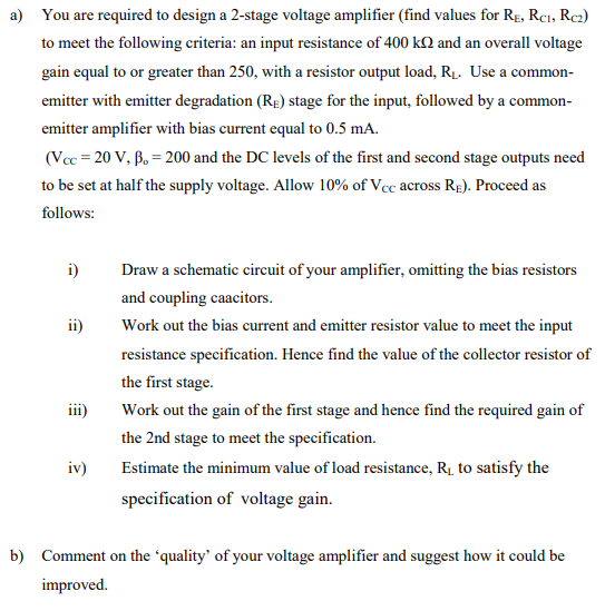
You are required to design a 2-stage voltage amplifier (find values for RE, RC1, RC2) to meet the following criteria: an input resistance of 400 kΩ and an overall voltage gain equal to or greater than 250, with a resistor output load, RL. Use a common-emitter with emitter degradation (RE) stage for the input, followed by a commonemitter amplifier with bias current equal to 0.5 mA. (VCC = 20 V, βo = 200 and the DC levels of the first and second stage outputs need to be set at half the supply voltage. Allow 10% of VCC across RE). Proceed as follows:
Homework Answers
Add Answer to:
You are required to design a 2-stage voltage amplifier (find values for RE, RC1, RC2) to meet the following criteria: an...
Perform a simple initial design of an ac coupled common-emitter amplifier with four resistor biasing and emitter by-pass...
 Perform a simple initial design of an ac coupled common-emitter
amplifier with
four resistor biasing and emitter by-pass capacitor, to have a
voltage gain of about
100, for the following conditions. Justify any approximations used.
(Assume Ic=1/300 A)
i)Transistor ac common-emitter gain, B, 100 ii) Supply voltage ofV0c-20V iii) Allow 10% Vcc across RE DC collector voltage of 10 V iv) v) DC current in the base bias resistors should be ten times greater than the DC base current. Assume...
Perform a simple initial design of an ac coupled common-emitter
amplifier with
four resistor biasing and emitter by-pass capacitor, to have a
voltage gain of about
100, for the following conditions. Justify any approximations used.
(Assume Ic=1/300 A)
i)Transistor ac common-emitter gain, B, 100 ii) Supply voltage ofV0c-20V iii) Allow 10% Vcc across RE DC collector voltage of 10 V iv) v) DC current in the base bias resistors should be ten times greater than the DC base current. Assume...
4. Design a npn BJT C-E amplifier circuit for the following specifications and given values: Voltage...
 4. Design a npn BJT C-E amplifier circuit for the following specifications and given values: Voltage Gain Input resistance Load resistance Supply voltage Av = -60 Ri = 5k92 RL = 6k2 Vcc= 16V Assume Re is fully bypassed. The input source internal resistance Rs = 0.12. B=120 and VBE= 0.65V. Draw the actual circuit and its ac equivalent circuit
1.0 kn. RE-390 Ω, r-15 Ω. and ßac-75. 5. For a common-emitter amplifier, Rc Assuming that Rg is completely bypassed at the operating frequency, the voltage gain is (a) 66.7 (d) 75 (b) 2.56 (c) 2....
 1.0 kn. RE-390 Ω, r-15 Ω. and ßac-75. 5. For a common-emitter amplifier, Rc Assuming that Rg is completely bypassed at the operating frequency, the voltage gain is (a) 66.7 (d) 75 (b) 2.56 (c) 2.47 6. In the circuit of Question 5, if the frequency is reduced to the point where Xctbypass) RE, the voltage gain (a) remains the same (b) is less (c) is greater 7. In a common-emitter amplifier with voltage-divider bias, Rimlbase) 68 k2, Ri 33...
Design a BJT amplifier based on the specifications provided in the table below. Your design shoul...
 THE STEPS TO DO SO:
Design a BJT amplifier based on the specifications provided in the table below. Your design should be insensitive to β variations, and both the input and the output should be AC coupled as in Fig. 1. Supply Voltage, Vcc Load Resistance, RL Transistor's Current Gain, β Relative Variation of lc for VBE-0.7 ± 0.1 V 0-to-Peak Output Swing, Vo Voltage Gain, A Input Resistance, R THD for 5kHz IV (0-to-peak) Sine Wave Output Voltage, V。S5%...
THE STEPS TO DO SO:
Design a BJT amplifier based on the specifications provided in the table below. Your design should be insensitive to β variations, and both the input and the output should be AC coupled as in Fig. 1. Supply Voltage, Vcc Load Resistance, RL Transistor's Current Gain, β Relative Variation of lc for VBE-0.7 ± 0.1 V 0-to-Peak Output Swing, Vo Voltage Gain, A Input Resistance, R THD for 5kHz IV (0-to-peak) Sine Wave Output Voltage, V。S5%...
FIND THE VALUES OF Rb1, Rb2, Re,Rc, rin , rout, overall gain and open circuit gain First, design a common emitter BJT a...
 FIND THE VALUES OF Rb1, Rb2, Re,Rc, rin , rout, overall gain and
open circuit gain
First, design a common emitter BJT amplifier Second, analyze the amplifier.( Avo, Gv, Rin, Rout) Third, compare your calculation with Multisim. Report must include comparison between your calculation & simulation results overall voltage gain, open circuit voltage gain, input resistance, and output resistance. This design project is not group work, must be done individually. Type your report. Design a discrete common emitter BJT amplifier.(Determine...
FIND THE VALUES OF Rb1, Rb2, Re,Rc, rin , rout, overall gain and
open circuit gain
First, design a common emitter BJT amplifier Second, analyze the amplifier.( Avo, Gv, Rin, Rout) Third, compare your calculation with Multisim. Report must include comparison between your calculation & simulation results overall voltage gain, open circuit voltage gain, input resistance, and output resistance. This design project is not group work, must be done individually. Type your report. Design a discrete common emitter BJT amplifier.(Determine...
Problem 2: BJT Small-Signal Voltage Amplifiers in the lectures, we covered in detail the analysis of an npn BJT amplifier that utilizes a single-supply DC biasing. In this problem, you will meet...
 Problem 2: BJT Small-Signal Voltage Amplifiers in the lectures, we covered in detail the analysis of an npn BJT amplifier that utilizes a single-supply DC biasing. In this problem, you will meet two additional amplifier architectures- one that is based on dual DC supplies combined with a DC current source, and the other that utilizes a pnp BJT with single-supply biasing. In both problems (below) you need to manually find the amplifier's Q-point (that is, the DC values of Ic...
4. Consider the BJT cascade amplifier shown below Vcc 18V R1 3.3ko 15uF r Vo RL...
 4. Consider the BJT cascade amplifier shown below Vcc 18V R1 3.3ko 15uF r Vo RL B 150 Rsa 500? 56k? Vi B 150 C1 CE 2.2k? a) Find the DC collector current (approximately the same in both transistors). b) Find the input impedance, output impedance, and no-load voltage gain. c) Find the Av, Avs, and Ai d) Estimate the lower cutoff frequency e) Why does this amplifier have better high-frequency performance thana common-emitter built using the same type of...
Fundamentals of Electronic Engineering Answer should be step by step and readable (clear handwriting) Given: •...
 Fundamentals of Electronic Engineering
Answer should be step by step and readable (clear
handwriting)
Given: • Power voltage: • Collector resistor: • Current amplification of BJT: • Source peak voltage: • Input/Output resistance: • The corner frequency: Vcc = 12V; Rc = 4k22; B = 100; Vs = 10mV; Rvs, RL = 1 ks2; f-3dB = 100Hz. Vec=12V w • Rc www R1 HE Сс CC2 RL + R2 RE CE Find: ? Bias quiescent point: Load line, Q-point, VcEQ,...
Fundamentals of Electronic Engineering
Answer should be step by step and readable (clear
handwriting)
Given: • Power voltage: • Collector resistor: • Current amplification of BJT: • Source peak voltage: • Input/Output resistance: • The corner frequency: Vcc = 12V; Rc = 4k22; B = 100; Vs = 10mV; Rvs, RL = 1 ks2; f-3dB = 100Hz. Vec=12V w • Rc www R1 HE Сс CC2 RL + R2 RE CE Find: ? Bias quiescent point: Load line, Q-point, VcEQ,...
I need help with 3.1 through 3.5 if possible . 3. For the two stage amplifier...
 I
need help with 3.1 through 3.5 if possible .
3. For the two stage amplifier Vcc-15V, Rsig-10Kohm, RL 2Kohm, First stage amplifier, RG 90Kohm, SV R3 RD115Kohm, RSI-2Kohm, gm 1mS and ro -20Kohm for transistor M1, Second stage amplifier, R3-40Kohm, . CI C4 7Kohm Lower corner frequency fi 3KHz. RSI Determine the configuration of the first and second stage amplifier. Configuration of first stage is Configuration of second stage is For Q3, find r,, gm. Rm"Re:9oka 1. - 2....
I
need help with 3.1 through 3.5 if possible .
3. For the two stage amplifier Vcc-15V, Rsig-10Kohm, RL 2Kohm, First stage amplifier, RG 90Kohm, SV R3 RD115Kohm, RSI-2Kohm, gm 1mS and ro -20Kohm for transistor M1, Second stage amplifier, R3-40Kohm, . CI C4 7Kohm Lower corner frequency fi 3KHz. RSI Determine the configuration of the first and second stage amplifier. Configuration of first stage is Configuration of second stage is For Q3, find r,, gm. Rm"Re:9oka 1. - 2....
Need to design and construct a two-stage amplifier with a total voltage gain of A =...
Need to design and construct a two-stage amplifier with a total voltage gain of A = A1 ∙ A2 = -Z where Z is 35. Let A1 be the gain of the first amplifier and A2 be the gain of the second amplifier. The output of Stage 1 becomes the input of Stage 2. Choose any suitable values |A|1 > 1 and |A2| >1 that you wish (Note that both gains must be strictly larger than 1. No buffers). Assume...
 Perform a simple initial design of an ac coupled common-emitter
amplifier with
four resistor biasing and emitter by-pass capacitor, to have a
voltage gain of about
100, for the following conditions. Justify any approximations used.
(Assume Ic=1/300 A)
i)Transistor ac common-emitter gain, B, 100 ii) Supply voltage ofV0c-20V iii) Allow 10% Vcc across RE DC collector voltage of 10 V iv) v) DC current in the base bias resistors should be ten times greater than the DC base current. Assume...
Perform a simple initial design of an ac coupled common-emitter
amplifier with
four resistor biasing and emitter by-pass capacitor, to have a
voltage gain of about
100, for the following conditions. Justify any approximations used.
(Assume Ic=1/300 A)
i)Transistor ac common-emitter gain, B, 100 ii) Supply voltage ofV0c-20V iii) Allow 10% Vcc across RE DC collector voltage of 10 V iv) v) DC current in the base bias resistors should be ten times greater than the DC base current. Assume...
 4. Design a npn BJT C-E amplifier circuit for the following specifications and given values: Voltage Gain Input resistance Load resistance Supply voltage Av = -60 Ri = 5k92 RL = 6k2 Vcc= 16V Assume Re is fully bypassed. The input source internal resistance Rs = 0.12. B=120 and VBE= 0.65V. Draw the actual circuit and its ac equivalent circuit
 1.0 kn. RE-390 Ω, r-15 Ω. and ßac-75. 5. For a common-emitter amplifier, Rc Assuming that Rg is completely bypassed at the operating frequency, the voltage gain is (a) 66.7 (d) 75 (b) 2.56 (c) 2.47 6. In the circuit of Question 5, if the frequency is reduced to the point where Xctbypass) RE, the voltage gain (a) remains the same (b) is less (c) is greater 7. In a common-emitter amplifier with voltage-divider bias, Rimlbase) 68 k2, Ri 33...
 THE STEPS TO DO SO:
Design a BJT amplifier based on the specifications provided in the table below. Your design should be insensitive to β variations, and both the input and the output should be AC coupled as in Fig. 1. Supply Voltage, Vcc Load Resistance, RL Transistor's Current Gain, β Relative Variation of lc for VBE-0.7 ± 0.1 V 0-to-Peak Output Swing, Vo Voltage Gain, A Input Resistance, R THD for 5kHz IV (0-to-peak) Sine Wave Output Voltage, V。S5%...
THE STEPS TO DO SO:
Design a BJT amplifier based on the specifications provided in the table below. Your design should be insensitive to β variations, and both the input and the output should be AC coupled as in Fig. 1. Supply Voltage, Vcc Load Resistance, RL Transistor's Current Gain, β Relative Variation of lc for VBE-0.7 ± 0.1 V 0-to-Peak Output Swing, Vo Voltage Gain, A Input Resistance, R THD for 5kHz IV (0-to-peak) Sine Wave Output Voltage, V。S5%...
 FIND THE VALUES OF Rb1, Rb2, Re,Rc, rin , rout, overall gain and
open circuit gain
First, design a common emitter BJT amplifier Second, analyze the amplifier.( Avo, Gv, Rin, Rout) Third, compare your calculation with Multisim. Report must include comparison between your calculation & simulation results overall voltage gain, open circuit voltage gain, input resistance, and output resistance. This design project is not group work, must be done individually. Type your report. Design a discrete common emitter BJT amplifier.(Determine...
FIND THE VALUES OF Rb1, Rb2, Re,Rc, rin , rout, overall gain and
open circuit gain
First, design a common emitter BJT amplifier Second, analyze the amplifier.( Avo, Gv, Rin, Rout) Third, compare your calculation with Multisim. Report must include comparison between your calculation & simulation results overall voltage gain, open circuit voltage gain, input resistance, and output resistance. This design project is not group work, must be done individually. Type your report. Design a discrete common emitter BJT amplifier.(Determine...
 Problem 2: BJT Small-Signal Voltage Amplifiers in the lectures, we covered in detail the analysis of an npn BJT amplifier that utilizes a single-supply DC biasing. In this problem, you will meet two additional amplifier architectures- one that is based on dual DC supplies combined with a DC current source, and the other that utilizes a pnp BJT with single-supply biasing. In both problems (below) you need to manually find the amplifier's Q-point (that is, the DC values of Ic...
 4. Consider the BJT cascade amplifier shown below Vcc 18V R1 3.3ko 15uF r Vo RL B 150 Rsa 500? 56k? Vi B 150 C1 CE 2.2k? a) Find the DC collector current (approximately the same in both transistors). b) Find the input impedance, output impedance, and no-load voltage gain. c) Find the Av, Avs, and Ai d) Estimate the lower cutoff frequency e) Why does this amplifier have better high-frequency performance thana common-emitter built using the same type of...
 Fundamentals of Electronic Engineering
Answer should be step by step and readable (clear
handwriting)
Given: • Power voltage: • Collector resistor: • Current amplification of BJT: • Source peak voltage: • Input/Output resistance: • The corner frequency: Vcc = 12V; Rc = 4k22; B = 100; Vs = 10mV; Rvs, RL = 1 ks2; f-3dB = 100Hz. Vec=12V w • Rc www R1 HE Сс CC2 RL + R2 RE CE Find: ? Bias quiescent point: Load line, Q-point, VcEQ,...
Fundamentals of Electronic Engineering
Answer should be step by step and readable (clear
handwriting)
Given: • Power voltage: • Collector resistor: • Current amplification of BJT: • Source peak voltage: • Input/Output resistance: • The corner frequency: Vcc = 12V; Rc = 4k22; B = 100; Vs = 10mV; Rvs, RL = 1 ks2; f-3dB = 100Hz. Vec=12V w • Rc www R1 HE Сс CC2 RL + R2 RE CE Find: ? Bias quiescent point: Load line, Q-point, VcEQ,...
 I
need help with 3.1 through 3.5 if possible .
3. For the two stage amplifier Vcc-15V, Rsig-10Kohm, RL 2Kohm, First stage amplifier, RG 90Kohm, SV R3 RD115Kohm, RSI-2Kohm, gm 1mS and ro -20Kohm for transistor M1, Second stage amplifier, R3-40Kohm, . CI C4 7Kohm Lower corner frequency fi 3KHz. RSI Determine the configuration of the first and second stage amplifier. Configuration of first stage is Configuration of second stage is For Q3, find r,, gm. Rm"Re:9oka 1. - 2....
I
need help with 3.1 through 3.5 if possible .
3. For the two stage amplifier Vcc-15V, Rsig-10Kohm, RL 2Kohm, First stage amplifier, RG 90Kohm, SV R3 RD115Kohm, RSI-2Kohm, gm 1mS and ro -20Kohm for transistor M1, Second stage amplifier, R3-40Kohm, . CI C4 7Kohm Lower corner frequency fi 3KHz. RSI Determine the configuration of the first and second stage amplifier. Configuration of first stage is Configuration of second stage is For Q3, find r,, gm. Rm"Re:9oka 1. - 2....
Most questions answered within 3 hours.
-
> Women’s pulse rates are normally distributed with a mean of
68.5 beats per minute and...
asked 1 minute ago -
Briefly describe an aspect of the strengths perspective that is
consistent with your own understanding of...
asked 3 minutes ago -
Step by step method of using Sparse Identification of Nonlinear
Dynamics (SINDy) to model your own...
asked 11 minutes ago -
3) What are the typical social structures in a global city?
asked 3 hours ago -
Luther Corporation
Consolidated Balance Sheet
December 31, 2019 and 2018 (in $ millions)
Assets
2019
2018...
asked 3 hours ago -
(Expected rate of return and risk) Carter Inc. is evaluating a
security. Calculate the investment’s expected...
asked 6 hours ago -
What specific indicators can point to lack of progress for
African Americans in American society?
asked 7 hours ago -
1-The Electrons in a beam are moving at 2.7×10⁸ m/s in an
electric field of 15000...
asked 7 hours ago -
A gas tank is a vertical cylinder. It has a radius of 1m, a
height of...
asked 7 hours ago -
Accent Software faces the following conditions. All of these
support Accent’s use of a market-penetration pricing...
asked 8 hours ago -
A mathematically inclined friend emails you the following
instructions: "Meet me in the cafeteria the first...
asked 8 hours ago -
A monopoly sells in two countries . The demand curves in the two
countries are p1...
asked 9 hours ago