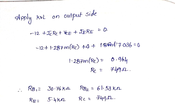
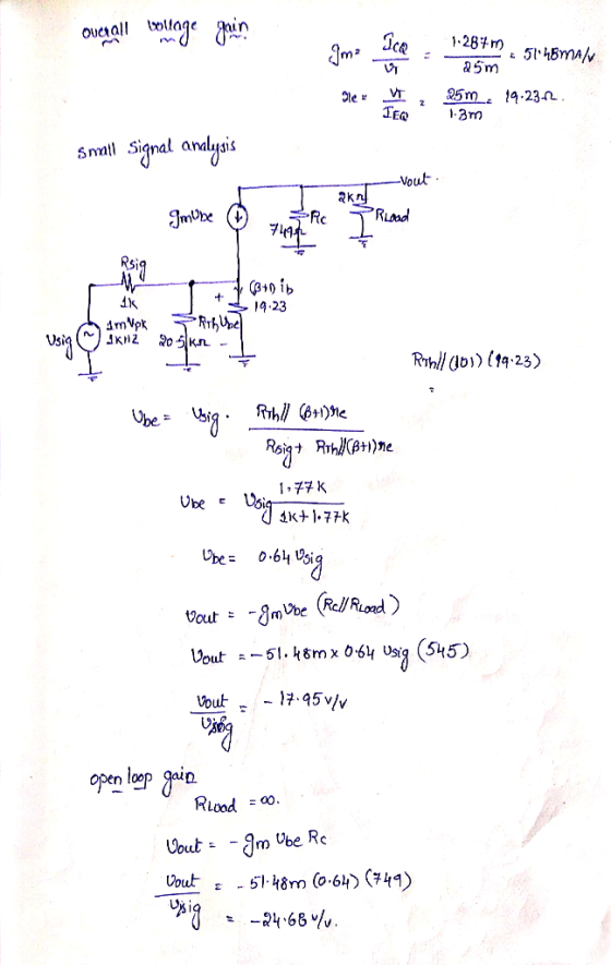
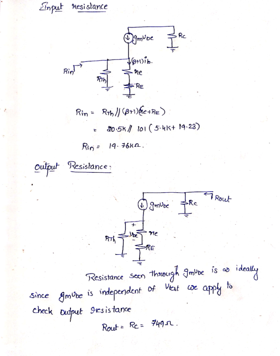
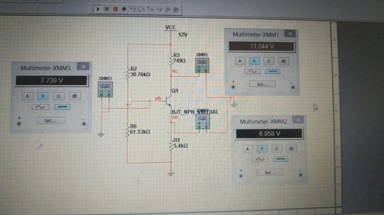
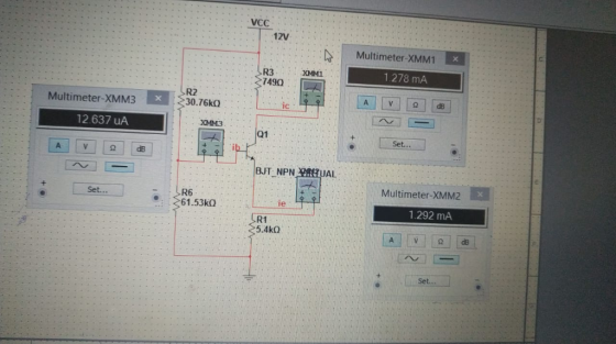
FIND THE VALUES OF Rb1, Rb2, Re,Rc, rin , rout, overall gain and open circuit gain
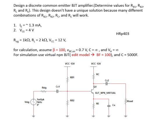
Design a discrete common emitter BJT amplifier.(Determine values for RB1, RB, Rc and RE). This design doesn't have a unique solution because many different combinations of RR1, RB2, Rc, and Re will work. 1. le -* 1.3 mA, 2. Vc-4 V HRp403 for calculation, assume β = 100,VBE.on-0.7 V, C = oo , and VA-00 For simulation use virtual npn BJT( edit model → BF = 100), and C = 5000F. VCC 12V VCC 12V RC RB1 Cc2 Cc1 Q1 Rsi BJT NPN VIRTUAL RB2 Rload Vsig1kHz 0° RE
Homework Answers
Add Answer to:
FIND THE VALUES OF Rb1, Rb2, Re,Rc, rin , rout, overall gain and open circuit gain First, design a common emitter BJT a...
VCC 15.0V RB1 RC Cc2 Vout Q1 4.7uF RL Cc1 Rsig 1kQ Vsig +100mVrms RB2 )50kHz...
 VCC 15.0V RB1 RC Cc2 Vout Q1 4.7uF RL Cc1 Rsig 1kQ Vsig +100mVrms RB2 )50kHz RE CE Fig. 1 npn BJT Common Emitter Amplifier I. (15 points) Assume β-100. Using the DC Model and assumptions, find VcEQ, loa-Show the model 2. (20 points) Using the small signal model, find Av, Rin, Rout. Show the model 3. (5 points) Determine the percent change in Av if ro is included in the analysis. Assume VA 1V
VCC 15.0V RB1 RC Cc2 Vout Q1 RL Cc1 Rsig 1HF Vsig 100mVrms 50kHz RB2 RE...
 VCC 15.0V RB1 RC Cc2 Vout Q1 RL Cc1 Rsig 1HF Vsig 100mVrms 50kHz RB2 RE CE Fig. 1 npn BJT Common Emitter Amplifier 1. (15 points) Assume 8-100. Using the DC Model and assumptions, find VCE Ica. Show the model. 2. (20 points) Using the small signal model, find A RinRoz. Show the model. 3. 5 ooints) Determine the percent change in Ay if ro is included in the analysis. Assume VA 1V
In a small signal voltage amplifier using a pnp transistor shown below, the voltage gain is 350.2. The value of a-0.95. Find the equivalent model emitter resistance re in Ohms if Rc-4.1K2. The BJT is...
 In a small signal voltage amplifier using a pnp transistor shown below, the voltage gain is 350.2. The value of a-0.95. Find the equivalent model emitter resistance re in Ohms if Rc-4.1K2. The BJT is operating at room temperature and VBE 0.7V RE-10K CCI vi Cc2 Rc
In a small signal voltage amplifier using a pnp transistor shown below, the voltage gain is 350.2. The value of a-0.95. Find the equivalent model emitter resistance re in Ohms if Rc-4.1K2. The...
In a small signal voltage amplifier using a pnp transistor shown below, the voltage gain is 350.2. The value of a-0.95. Find the equivalent model emitter resistance re in Ohms if Rc-4.1K2. The BJT is operating at room temperature and VBE 0.7V RE-10K CCI vi Cc2 Rc
In a small signal voltage amplifier using a pnp transistor shown below, the voltage gain is 350.2. The value of a-0.95. Find the equivalent model emitter resistance re in Ohms if Rc-4.1K2. The...
I have constructed this NPN Common-Emitter circuit in multisim and am asked to "Perform AC Simula...
 I have constructed this NPN Common-Emitter circuit in multisim
and am asked to "Perform AC Simulation to obtain
Av(gain), Ri, and Ro". How could I
do that? Please list out the steps/instructions to do so.
VCC 5.0V RB1 RC 1120Ω Vo C1 Q1 2N3904 1F Vi C2 1Vpk 1kHz 0° RB2 1F RE 400Ω RG 35Ω
VCC 5.0V RB1 RC 1120Ω Vo C1 Q1 2N3904 1F Vi C2 1Vpk 1kHz 0° RB2 1F RE 400Ω RG 35Ω
I have constructed this NPN Common-Emitter circuit in multisim
and am asked to "Perform AC Simulation to obtain
Av(gain), Ri, and Ro". How could I
do that? Please list out the steps/instructions to do so.
VCC 5.0V RB1 RC 1120Ω Vo C1 Q1 2N3904 1F Vi C2 1Vpk 1kHz 0° RB2 1F RE 400Ω RG 35Ω
VCC 5.0V RB1 RC 1120Ω Vo C1 Q1 2N3904 1F Vi C2 1Vpk 1kHz 0° RB2 1F RE 400Ω RG 35Ω
(a) Design the circuit (Find values for Rc, Rei and Rez) to amplify a 12mV sinusoidal...
 (a) Design the circuit (Find values for Rc, Rei and Rez) to amplify a 12mV sinusoidal signal from a microphone to a 0.4 V sinusoidal output signal, and make le = 0.2 mA. (20 points) (6) Draw complete small signal equivalent circuit of the amplifier. Clearly label all components. (Spoints) (c) Find values of input resistance (Rin), output resistance (Rout), and open circuit voltage gain ( Avo). (20 points) Assume B = 100, VBE.ON=0.7V, VA=00, and capacitors are very large...
Need some help for this Problem 1: Consider the circuit below. Vcc = 12V, R31 =...
 Need some help for this
Problem 1: Consider the circuit below. Vcc = 12V, R31 = 120k12, RB2 = 40 k12, R33 = 120 k12, R34 = 20k12, Rei 3k12, Re2 = 1k12, Rc2= 10 kN, Rcz = 0 and B = 50. a. Calculate the collector current and emitter voltage for both transistors. Neglect Early effect b. Draw the small signal equivalent circuit. c. Calculate Rin2, Rin, Rout d. Calculate the overall gain with load of the amplifier if...
Need some help for this
Problem 1: Consider the circuit below. Vcc = 12V, R31 = 120k12, RB2 = 40 k12, R33 = 120 k12, R34 = 20k12, Rei 3k12, Re2 = 1k12, Rc2= 10 kN, Rcz = 0 and B = 50. a. Calculate the collector current and emitter voltage for both transistors. Neglect Early effect b. Draw the small signal equivalent circuit. c. Calculate Rin2, Rin, Rout d. Calculate the overall gain with load of the amplifier if...
please I need details l and....Debate Club | Offic A) Theoretical Design Design a common emitter BJT amplifier with the following requirements: -Rin-10 K2, and Ro-45 ㏀ (Neglect the Early voltage...
 please I need details
l and....Debate Club | Offic A) Theoretical Design Design a common emitter BJT amplifier with the following requirements: -Rin-10 K2, and Ro-45 ㏀ (Neglect the Early voltage Effect) Vo/Vsig- Gv-40 VIV or 32 dB " VCC-9 V V, IC-1mA, VCE-3.25V and β-100 RL-40 kQ, Rsige I ka, R 1-3R2, and C1-C2-1 μF Voc RC C2 R1 Rsig C1 RL R2 RE B) Verify your design using Orcad Capture Pspice by doing 1) AC sweep (frequency response):...
please I need details
l and....Debate Club | Offic A) Theoretical Design Design a common emitter BJT amplifier with the following requirements: -Rin-10 K2, and Ro-45 ㏀ (Neglect the Early voltage Effect) Vo/Vsig- Gv-40 VIV or 32 dB " VCC-9 V V, IC-1mA, VCE-3.25V and β-100 RL-40 kQ, Rsige I ka, R 1-3R2, and C1-C2-1 μF Voc RC C2 R1 Rsig C1 RL R2 RE B) Verify your design using Orcad Capture Pspice by doing 1) AC sweep (frequency response):...
6.5 BI C2 Cl sig in 0 Design the bias circuit of the CE amplifier shown...
 6.5 BI C2 Cl sig in 0 Design the bias circuit of the CE amplifier shown to obtain IE= 0.5 mA and Vc= +6 V. Design for a dc voltage at the base of 5 V and a current through RB2 of 50 μΑ. Let Vcc-+15 V, β-100, and VBE 0.7 V. a) Specify the values of RBi, RB2, RE, and Rc b) Also give the values of the BJT small-signal parameters gm, rr , and ro at the bias...
1. Consider the Common-Emitter BJT amplifier circuit, shown below. VD VOD BJT Parameters: B=99 A/A i=0...
 1. Consider the Common-Emitter BJT amplifier circuit, shown below. VD VOD BJT Parameters: B=99 A/A i=0 RE Co Circuit Parameters: Ca Cc2 = 0 F Car = OF R = 2022 R = 2002 R1 = 25.8 k22 Ry2 = 51.6 ks V = 15 V VEE=0 V Сct Active Mode: Va >0.2 V Vwx=0.7V Ic=B1, Ic=al, 1 R2 3 SRCA a) Find the open-circuit voltage gain, Ave, of this amplifier circuit. Verify your assumptions. b) Compute the input resistance,...
1. Design the common-emitter amplifier in Fig. 4(a) with the following specifications: Supply Vol...
 Figure 4. (a)
1. Design the common-emitter amplifier in Fig. 4(a) with the following specifications: Supply Voltage, Vcc 0-to-Peak Output Swing, V Voltage Gain, A. Input Resistance, R Output Resistance, Ro THD for 5kHz 1 V (0-to-peak) Sine Wave Output Voltage, V Relative Variation of Ic for VBE 0.7t 0.1V Transistor's Current Gain, β 5V 25 1.8kS2 4% 10% 100 Show your design procedure and all your calculations. Your design should be insensitive to B variations. Vcc RB1 Rc 0...
Figure 4. (a)
1. Design the common-emitter amplifier in Fig. 4(a) with the following specifications: Supply Voltage, Vcc 0-to-Peak Output Swing, V Voltage Gain, A. Input Resistance, R Output Resistance, Ro THD for 5kHz 1 V (0-to-peak) Sine Wave Output Voltage, V Relative Variation of Ic for VBE 0.7t 0.1V Transistor's Current Gain, β 5V 25 1.8kS2 4% 10% 100 Show your design procedure and all your calculations. Your design should be insensitive to B variations. Vcc RB1 Rc 0...
 VCC 15.0V RB1 RC Cc2 Vout Q1 4.7uF RL Cc1 Rsig 1kQ Vsig +100mVrms RB2 )50kHz RE CE Fig. 1 npn BJT Common Emitter Amplifier I. (15 points) Assume β-100. Using the DC Model and assumptions, find VcEQ, loa-Show the model 2. (20 points) Using the small signal model, find Av, Rin, Rout. Show the model 3. (5 points) Determine the percent change in Av if ro is included in the analysis. Assume VA 1V
 VCC 15.0V RB1 RC Cc2 Vout Q1 RL Cc1 Rsig 1HF Vsig 100mVrms 50kHz RB2 RE CE Fig. 1 npn BJT Common Emitter Amplifier 1. (15 points) Assume 8-100. Using the DC Model and assumptions, find VCE Ica. Show the model. 2. (20 points) Using the small signal model, find A RinRoz. Show the model. 3. 5 ooints) Determine the percent change in Ay if ro is included in the analysis. Assume VA 1V
 In a small signal voltage amplifier using a pnp transistor shown below, the voltage gain is 350.2. The value of a-0.95. Find the equivalent model emitter resistance re in Ohms if Rc-4.1K2. The BJT is operating at room temperature and VBE 0.7V RE-10K CCI vi Cc2 Rc
In a small signal voltage amplifier using a pnp transistor shown below, the voltage gain is 350.2. The value of a-0.95. Find the equivalent model emitter resistance re in Ohms if Rc-4.1K2. The...
In a small signal voltage amplifier using a pnp transistor shown below, the voltage gain is 350.2. The value of a-0.95. Find the equivalent model emitter resistance re in Ohms if Rc-4.1K2. The BJT is operating at room temperature and VBE 0.7V RE-10K CCI vi Cc2 Rc
In a small signal voltage amplifier using a pnp transistor shown below, the voltage gain is 350.2. The value of a-0.95. Find the equivalent model emitter resistance re in Ohms if Rc-4.1K2. The...
 I have constructed this NPN Common-Emitter circuit in multisim
and am asked to "Perform AC Simulation to obtain
Av(gain), Ri, and Ro". How could I
do that? Please list out the steps/instructions to do so.
VCC 5.0V RB1 RC 1120Ω Vo C1 Q1 2N3904 1F Vi C2 1Vpk 1kHz 0° RB2 1F RE 400Ω RG 35Ω
VCC 5.0V RB1 RC 1120Ω Vo C1 Q1 2N3904 1F Vi C2 1Vpk 1kHz 0° RB2 1F RE 400Ω RG 35Ω
I have constructed this NPN Common-Emitter circuit in multisim
and am asked to "Perform AC Simulation to obtain
Av(gain), Ri, and Ro". How could I
do that? Please list out the steps/instructions to do so.
VCC 5.0V RB1 RC 1120Ω Vo C1 Q1 2N3904 1F Vi C2 1Vpk 1kHz 0° RB2 1F RE 400Ω RG 35Ω
VCC 5.0V RB1 RC 1120Ω Vo C1 Q1 2N3904 1F Vi C2 1Vpk 1kHz 0° RB2 1F RE 400Ω RG 35Ω
 (a) Design the circuit (Find values for Rc, Rei and Rez) to amplify a 12mV sinusoidal signal from a microphone to a 0.4 V sinusoidal output signal, and make le = 0.2 mA. (20 points) (6) Draw complete small signal equivalent circuit of the amplifier. Clearly label all components. (Spoints) (c) Find values of input resistance (Rin), output resistance (Rout), and open circuit voltage gain ( Avo). (20 points) Assume B = 100, VBE.ON=0.7V, VA=00, and capacitors are very large...
 Need some help for this
Problem 1: Consider the circuit below. Vcc = 12V, R31 = 120k12, RB2 = 40 k12, R33 = 120 k12, R34 = 20k12, Rei 3k12, Re2 = 1k12, Rc2= 10 kN, Rcz = 0 and B = 50. a. Calculate the collector current and emitter voltage for both transistors. Neglect Early effect b. Draw the small signal equivalent circuit. c. Calculate Rin2, Rin, Rout d. Calculate the overall gain with load of the amplifier if...
Need some help for this
Problem 1: Consider the circuit below. Vcc = 12V, R31 = 120k12, RB2 = 40 k12, R33 = 120 k12, R34 = 20k12, Rei 3k12, Re2 = 1k12, Rc2= 10 kN, Rcz = 0 and B = 50. a. Calculate the collector current and emitter voltage for both transistors. Neglect Early effect b. Draw the small signal equivalent circuit. c. Calculate Rin2, Rin, Rout d. Calculate the overall gain with load of the amplifier if...
 please I need details
l and....Debate Club | Offic A) Theoretical Design Design a common emitter BJT amplifier with the following requirements: -Rin-10 K2, and Ro-45 ㏀ (Neglect the Early voltage Effect) Vo/Vsig- Gv-40 VIV or 32 dB " VCC-9 V V, IC-1mA, VCE-3.25V and β-100 RL-40 kQ, Rsige I ka, R 1-3R2, and C1-C2-1 μF Voc RC C2 R1 Rsig C1 RL R2 RE B) Verify your design using Orcad Capture Pspice by doing 1) AC sweep (frequency response):...
please I need details
l and....Debate Club | Offic A) Theoretical Design Design a common emitter BJT amplifier with the following requirements: -Rin-10 K2, and Ro-45 ㏀ (Neglect the Early voltage Effect) Vo/Vsig- Gv-40 VIV or 32 dB " VCC-9 V V, IC-1mA, VCE-3.25V and β-100 RL-40 kQ, Rsige I ka, R 1-3R2, and C1-C2-1 μF Voc RC C2 R1 Rsig C1 RL R2 RE B) Verify your design using Orcad Capture Pspice by doing 1) AC sweep (frequency response):...
 6.5 BI C2 Cl sig in 0 Design the bias circuit of the CE amplifier shown to obtain IE= 0.5 mA and Vc= +6 V. Design for a dc voltage at the base of 5 V and a current through RB2 of 50 μΑ. Let Vcc-+15 V, β-100, and VBE 0.7 V. a) Specify the values of RBi, RB2, RE, and Rc b) Also give the values of the BJT small-signal parameters gm, rr , and ro at the bias...
 1. Consider the Common-Emitter BJT amplifier circuit, shown below. VD VOD BJT Parameters: B=99 A/A i=0 RE Co Circuit Parameters: Ca Cc2 = 0 F Car = OF R = 2022 R = 2002 R1 = 25.8 k22 Ry2 = 51.6 ks V = 15 V VEE=0 V Сct Active Mode: Va >0.2 V Vwx=0.7V Ic=B1, Ic=al, 1 R2 3 SRCA a) Find the open-circuit voltage gain, Ave, of this amplifier circuit. Verify your assumptions. b) Compute the input resistance,...
 Figure 4. (a)
1. Design the common-emitter amplifier in Fig. 4(a) with the following specifications: Supply Voltage, Vcc 0-to-Peak Output Swing, V Voltage Gain, A. Input Resistance, R Output Resistance, Ro THD for 5kHz 1 V (0-to-peak) Sine Wave Output Voltage, V Relative Variation of Ic for VBE 0.7t 0.1V Transistor's Current Gain, β 5V 25 1.8kS2 4% 10% 100 Show your design procedure and all your calculations. Your design should be insensitive to B variations. Vcc RB1 Rc 0...
Figure 4. (a)
1. Design the common-emitter amplifier in Fig. 4(a) with the following specifications: Supply Voltage, Vcc 0-to-Peak Output Swing, V Voltage Gain, A. Input Resistance, R Output Resistance, Ro THD for 5kHz 1 V (0-to-peak) Sine Wave Output Voltage, V Relative Variation of Ic for VBE 0.7t 0.1V Transistor's Current Gain, β 5V 25 1.8kS2 4% 10% 100 Show your design procedure and all your calculations. Your design should be insensitive to B variations. Vcc RB1 Rc 0...
Most questions answered within 3 hours.
-
If a block of Si is doped with 10^17 Boron atom/cm^3 and 5X10^16
Arsenic atoms/cm^3,
(a)...
asked 1 minute ago -
Why would natural selection not minimize costs (in the form of
symptoms) of evolved defenses? (choose...
asked 19 minutes ago -
What is true about a critical task?
Latest finish time - latest start time = 0...
asked 22 minutes ago -
A company uses a
process costing system. Its Assembly Department's beginning
inventory consisted of 56,800 units,...
asked 22 minutes ago -
a
sealed glass cylinder contains 325 g of N2 gas at 1.02 atm at 20 c....
asked 26 minutes ago -
The main difference between an equity and a nonequity alliance
is that
A
equity alliances are...
asked 24 minutes ago -
Need help with this, in JAVA, using netbeans. A
complete response will receive a positive comment...
asked 33 minutes ago -
An imprest petty cash fund of $600 was established for minor
disbursements. At the end of...
asked 38 minutes ago -
Sharpe Cutter is a small company that produces specialty knives
for paper cutting machinery. The annual...
asked 42 minutes ago -
Calculating the Ka of a weak acid from
pH:
The pH of a 0.68M solution of...
asked 43 minutes ago -
1.What process is pushing back against gravity in the very
center (the core) of sun-like stars?...
asked 1 hour ago -
This question is from the textbook "Python for ArcGIS" by Laura
Tateosian:
Write a script "triangles.py"...
asked 1 hour ago