
Figure 4. (a)
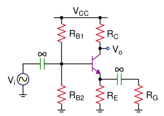
Vcc RB1 Rc 0 RG
Homework Answers


Add Answer to:
1. Design the common-emitter amplifier in Fig. 4(a) with the following specifications: Supply Vol...
Design a BJT amplifier based on the specifications provided in the table below. Your design shoul...
 THE STEPS TO DO SO:
Design a BJT amplifier based on the specifications provided in the table below. Your design should be insensitive to β variations, and both the input and the output should be AC coupled as in Fig. 1. Supply Voltage, Vcc Load Resistance, RL Transistor's Current Gain, β Relative Variation of lc for VBE-0.7 ± 0.1 V 0-to-Peak Output Swing, Vo Voltage Gain, A Input Resistance, R THD for 5kHz IV (0-to-peak) Sine Wave Output Voltage, V。S5%...
THE STEPS TO DO SO:
Design a BJT amplifier based on the specifications provided in the table below. Your design should be insensitive to β variations, and both the input and the output should be AC coupled as in Fig. 1. Supply Voltage, Vcc Load Resistance, RL Transistor's Current Gain, β Relative Variation of lc for VBE-0.7 ± 0.1 V 0-to-Peak Output Swing, Vo Voltage Gain, A Input Resistance, R THD for 5kHz IV (0-to-peak) Sine Wave Output Voltage, V。S5%...
FIND THE VALUES OF Rb1, Rb2, Re,Rc, rin , rout, overall gain and open circuit gain First, design a common emitter BJT a...
 FIND THE VALUES OF Rb1, Rb2, Re,Rc, rin , rout, overall gain and
open circuit gain
First, design a common emitter BJT amplifier Second, analyze the amplifier.( Avo, Gv, Rin, Rout) Third, compare your calculation with Multisim. Report must include comparison between your calculation & simulation results overall voltage gain, open circuit voltage gain, input resistance, and output resistance. This design project is not group work, must be done individually. Type your report. Design a discrete common emitter BJT amplifier.(Determine...
FIND THE VALUES OF Rb1, Rb2, Re,Rc, rin , rout, overall gain and
open circuit gain
First, design a common emitter BJT amplifier Second, analyze the amplifier.( Avo, Gv, Rin, Rout) Third, compare your calculation with Multisim. Report must include comparison between your calculation & simulation results overall voltage gain, open circuit voltage gain, input resistance, and output resistance. This design project is not group work, must be done individually. Type your report. Design a discrete common emitter BJT amplifier.(Determine...
[1] The circuit diagram on the left below is a common emitter amplifier. It is the...
 [1] The circuit diagram on the left below is a common emitter amplifier. It is the full complement of components for this type of amplifier ready for AC analysis. This amplifier will be discussed in lecture prior to the lab exercises. However, with the circuit including only Rc. RE, Ri, and R2 as shown in the figure on the right, proceed with the design for a DC operating point of the common emitter amplifier. The following parameters are given: Vcc...
Design a common emitter (voltage amp) PNP amplifier with a voltage gain of 25, VCC =...
Design a common emitter (voltage amp) PNP amplifier with a voltage gain of 25, VCC = +15 V, and IC = 0.25 mA. Bias the collector at 0.5VCC. (Coupling capacitor selection is optional.)
Design the inductively coupled common emitter (CE) amplifier shown in Fig. for Q. 7(a) to drive...
 Design the inductively coupled common emitter (CE) amplifier
shown in Fig. for Q. 7(a) to drive a 2 kQ. load with Vcc = 12 V,
VBE = 0.7 Y, β = 200, Rin = 4 kQ. and Av = -10.
Determine the current gain Ai and power delivered to the load
Po.
[Hint: Draw the small signal equivalent circuit and use Rg = 0.1BRę, where R, =R,||R, ). -- -- oom. . b 09 PR Vo - . Fig. for...
Design the inductively coupled common emitter (CE) amplifier
shown in Fig. for Q. 7(a) to drive a 2 kQ. load with Vcc = 12 V,
VBE = 0.7 Y, β = 200, Rin = 4 kQ. and Av = -10.
Determine the current gain Ai and power delivered to the load
Po.
[Hint: Draw the small signal equivalent circuit and use Rg = 0.1BRę, where R, =R,||R, ). -- -- oom. . b 09 PR Vo - . Fig. for...
Perform a simple initial design of an ac coupled common-emitter amplifier with four resistor biasing and emitter by-pass...
 Perform a simple initial design of an ac coupled common-emitter
amplifier with
four resistor biasing and emitter by-pass capacitor, to have a
voltage gain of about
100, for the following conditions. Justify any approximations used.
(Assume Ic=1/300 A)
i)Transistor ac common-emitter gain, B, 100 ii) Supply voltage ofV0c-20V iii) Allow 10% Vcc across RE DC collector voltage of 10 V iv) v) DC current in the base bias resistors should be ten times greater than the DC base current. Assume...
Perform a simple initial design of an ac coupled common-emitter
amplifier with
four resistor biasing and emitter by-pass capacitor, to have a
voltage gain of about
100, for the following conditions. Justify any approximations used.
(Assume Ic=1/300 A)
i)Transistor ac common-emitter gain, B, 100 ii) Supply voltage ofV0c-20V iii) Allow 10% Vcc across RE DC collector voltage of 10 V iv) v) DC current in the base bias resistors should be ten times greater than the DC base current. Assume...
Shown below is a single stage common emitter amplifier with a unipolar dc power supply using an 2...
 Shown below is a single stage common emitter amplifier with a unipolar dc power supply using an 2N3904 NPN BJT as the active device. It is specified that V+ 40 V, C1 C2CE 100uF, Ro-7.5 k2, REi-5.1kS2, and Ri - 36k52. Design the circuit so that the dc collector current is 2 mA and the magnitude of the small-signal midband voltage gain is 32.3. For the design calculations assume that the base-to- emitter dc voltage drop is 0.65 V, the...
Design a common emitter amplifier of nominal gain g = −10 to work at f =...
Design a common emitter amplifier of nominal gain g = −10 to work at f = 100 kHz. Let the supply voltages VCC = ±12 V. Center the output voltage as best you can. Use capacitive coupling and set the quiescent current at 1.0 mA.
Vsig = 10mV*sin(2Kπ) The circuit above is a common-emitter amplifier. Given the parameters in the circuit,...
 Vsig = 10mV*sin(2Kπ)
The circuit above is a common-emitter amplifier. Given the
parameters in the circuit,
1. If Rb1=10KΩ, Calculate Rb2, Ib, Ic, Ie, Re, transconductance
(gm), Current through Rb1 (I_rb1), and Current through Rb2(I_rb2),
Vb, Vc, Ve, Vce. Also, calculate Rc to achieve a voltage gain Av =
- 100 V/
(If Rb1 value does not match up, then choose your resistor
value for Rb1.)
2. If the amplitude of Vsig keeps increasing, at what amplitude
of the input...
Vsig = 10mV*sin(2Kπ)
The circuit above is a common-emitter amplifier. Given the
parameters in the circuit,
1. If Rb1=10KΩ, Calculate Rb2, Ib, Ic, Ie, Re, transconductance
(gm), Current through Rb1 (I_rb1), and Current through Rb2(I_rb2),
Vb, Vc, Ve, Vce. Also, calculate Rc to achieve a voltage gain Av =
- 100 V/
(If Rb1 value does not match up, then choose your resistor
value for Rb1.)
2. If the amplitude of Vsig keeps increasing, at what amplitude
of the input...
You are required to design a 2-stage voltage amplifier (find values for RE, RC1, RC2) to meet the following criteria: an...
 You are required to design a 2-stage voltage amplifier (find
values for RE, RC1, RC2) to meet the following criteria: an input
resistance of 400 kΩ and an overall voltage gain equal to or
greater than 250, with a resistor output load, RL. Use a
common-emitter with emitter degradation (RE) stage for the input,
followed by a commonemitter amplifier with bias current equal to
0.5 mA. (VCC = 20 V, βo = 200 and the DC levels of the first...
You are required to design a 2-stage voltage amplifier (find
values for RE, RC1, RC2) to meet the following criteria: an input
resistance of 400 kΩ and an overall voltage gain equal to or
greater than 250, with a resistor output load, RL. Use a
common-emitter with emitter degradation (RE) stage for the input,
followed by a commonemitter amplifier with bias current equal to
0.5 mA. (VCC = 20 V, βo = 200 and the DC levels of the first...
 THE STEPS TO DO SO:
Design a BJT amplifier based on the specifications provided in the table below. Your design should be insensitive to β variations, and both the input and the output should be AC coupled as in Fig. 1. Supply Voltage, Vcc Load Resistance, RL Transistor's Current Gain, β Relative Variation of lc for VBE-0.7 ± 0.1 V 0-to-Peak Output Swing, Vo Voltage Gain, A Input Resistance, R THD for 5kHz IV (0-to-peak) Sine Wave Output Voltage, V。S5%...
THE STEPS TO DO SO:
Design a BJT amplifier based on the specifications provided in the table below. Your design should be insensitive to β variations, and both the input and the output should be AC coupled as in Fig. 1. Supply Voltage, Vcc Load Resistance, RL Transistor's Current Gain, β Relative Variation of lc for VBE-0.7 ± 0.1 V 0-to-Peak Output Swing, Vo Voltage Gain, A Input Resistance, R THD for 5kHz IV (0-to-peak) Sine Wave Output Voltage, V。S5%...
 FIND THE VALUES OF Rb1, Rb2, Re,Rc, rin , rout, overall gain and
open circuit gain
First, design a common emitter BJT amplifier Second, analyze the amplifier.( Avo, Gv, Rin, Rout) Third, compare your calculation with Multisim. Report must include comparison between your calculation & simulation results overall voltage gain, open circuit voltage gain, input resistance, and output resistance. This design project is not group work, must be done individually. Type your report. Design a discrete common emitter BJT amplifier.(Determine...
FIND THE VALUES OF Rb1, Rb2, Re,Rc, rin , rout, overall gain and
open circuit gain
First, design a common emitter BJT amplifier Second, analyze the amplifier.( Avo, Gv, Rin, Rout) Third, compare your calculation with Multisim. Report must include comparison between your calculation & simulation results overall voltage gain, open circuit voltage gain, input resistance, and output resistance. This design project is not group work, must be done individually. Type your report. Design a discrete common emitter BJT amplifier.(Determine...
 [1] The circuit diagram on the left below is a common emitter amplifier. It is the full complement of components for this type of amplifier ready for AC analysis. This amplifier will be discussed in lecture prior to the lab exercises. However, with the circuit including only Rc. RE, Ri, and R2 as shown in the figure on the right, proceed with the design for a DC operating point of the common emitter amplifier. The following parameters are given: Vcc...
 Design the inductively coupled common emitter (CE) amplifier
shown in Fig. for Q. 7(a) to drive a 2 kQ. load with Vcc = 12 V,
VBE = 0.7 Y, β = 200, Rin = 4 kQ. and Av = -10.
Determine the current gain Ai and power delivered to the load
Po.
[Hint: Draw the small signal equivalent circuit and use Rg = 0.1BRę, where R, =R,||R, ). -- -- oom. . b 09 PR Vo - . Fig. for...
Design the inductively coupled common emitter (CE) amplifier
shown in Fig. for Q. 7(a) to drive a 2 kQ. load with Vcc = 12 V,
VBE = 0.7 Y, β = 200, Rin = 4 kQ. and Av = -10.
Determine the current gain Ai and power delivered to the load
Po.
[Hint: Draw the small signal equivalent circuit and use Rg = 0.1BRę, where R, =R,||R, ). -- -- oom. . b 09 PR Vo - . Fig. for...
 Perform a simple initial design of an ac coupled common-emitter
amplifier with
four resistor biasing and emitter by-pass capacitor, to have a
voltage gain of about
100, for the following conditions. Justify any approximations used.
(Assume Ic=1/300 A)
i)Transistor ac common-emitter gain, B, 100 ii) Supply voltage ofV0c-20V iii) Allow 10% Vcc across RE DC collector voltage of 10 V iv) v) DC current in the base bias resistors should be ten times greater than the DC base current. Assume...
Perform a simple initial design of an ac coupled common-emitter
amplifier with
four resistor biasing and emitter by-pass capacitor, to have a
voltage gain of about
100, for the following conditions. Justify any approximations used.
(Assume Ic=1/300 A)
i)Transistor ac common-emitter gain, B, 100 ii) Supply voltage ofV0c-20V iii) Allow 10% Vcc across RE DC collector voltage of 10 V iv) v) DC current in the base bias resistors should be ten times greater than the DC base current. Assume...
 Shown below is a single stage common emitter amplifier with a unipolar dc power supply using an 2N3904 NPN BJT as the active device. It is specified that V+ 40 V, C1 C2CE 100uF, Ro-7.5 k2, REi-5.1kS2, and Ri - 36k52. Design the circuit so that the dc collector current is 2 mA and the magnitude of the small-signal midband voltage gain is 32.3. For the design calculations assume that the base-to- emitter dc voltage drop is 0.65 V, the...
 Vsig = 10mV*sin(2Kπ)
The circuit above is a common-emitter amplifier. Given the
parameters in the circuit,
1. If Rb1=10KΩ, Calculate Rb2, Ib, Ic, Ie, Re, transconductance
(gm), Current through Rb1 (I_rb1), and Current through Rb2(I_rb2),
Vb, Vc, Ve, Vce. Also, calculate Rc to achieve a voltage gain Av =
- 100 V/
(If Rb1 value does not match up, then choose your resistor
value for Rb1.)
2. If the amplitude of Vsig keeps increasing, at what amplitude
of the input...
Vsig = 10mV*sin(2Kπ)
The circuit above is a common-emitter amplifier. Given the
parameters in the circuit,
1. If Rb1=10KΩ, Calculate Rb2, Ib, Ic, Ie, Re, transconductance
(gm), Current through Rb1 (I_rb1), and Current through Rb2(I_rb2),
Vb, Vc, Ve, Vce. Also, calculate Rc to achieve a voltage gain Av =
- 100 V/
(If Rb1 value does not match up, then choose your resistor
value for Rb1.)
2. If the amplitude of Vsig keeps increasing, at what amplitude
of the input...
 You are required to design a 2-stage voltage amplifier (find
values for RE, RC1, RC2) to meet the following criteria: an input
resistance of 400 kΩ and an overall voltage gain equal to or
greater than 250, with a resistor output load, RL. Use a
common-emitter with emitter degradation (RE) stage for the input,
followed by a commonemitter amplifier with bias current equal to
0.5 mA. (VCC = 20 V, βo = 200 and the DC levels of the first...
You are required to design a 2-stage voltage amplifier (find
values for RE, RC1, RC2) to meet the following criteria: an input
resistance of 400 kΩ and an overall voltage gain equal to or
greater than 250, with a resistor output load, RL. Use a
common-emitter with emitter degradation (RE) stage for the input,
followed by a commonemitter amplifier with bias current equal to
0.5 mA. (VCC = 20 V, βo = 200 and the DC levels of the first...
Most questions answered within 3 hours.
-
Investor company owns 35% of investee company voting stock and
accounts for the investment under the...
asked 57 minutes ago -
The number of major faults on a randomly chosen 1 km stretch of
highway has a...
asked 1 hour ago -
Consider the competitive environment of Starbuck's, Progressive
Insurance, a manufacturing firm with low turnover, or a...
asked 2 hours ago -
3. Gains from trade
Consider two neighbouring island countries called Euphoria and
Contente. They each have...
asked 4 hours ago -
A business executive has the option to invest money in two
plans: Plan A guarantees that...
asked 6 hours ago -
Hello, can someone please help me answer this question?
How much heat is absorbed by a...
asked 6 hours ago -
. A marketing researcher conducted a survey of 25 shoppers
randomly selected at the local mall...
asked 6 hours ago -
Create an comprehensive response to the
following:
Antimicrobial agents work on a multitude of microbes (bacteria,...
asked 6 hours ago -
6.13 LAB: Step counter. Section 6.3.
A pedometer treats walking 2,000 steps as walking 1 mile....
asked 6 hours ago -
(14.2) A block of mass m = 10 kg riding on a frictionless
horizontal plane is...
asked 6 hours ago -
Use any search engine to search for articles about Starbucks
partnership with Tata Companies in India...
asked 6 hours ago -
Let’s say that for some reason Bank Excess Reserves suddenly
increase sharply. What effect would this...
asked 6 hours ago