Design the inductively coupled common emitter (CE) amplifier
shown in Fig. for Q. 7(a) to drive a 2 kQ. load with Vcc = 12 V,
VBE = 0.7 Y, β = 200, Rin = 4 kQ. and Av = -10.
Determine the current gain Ai and power delivered to the load
Po.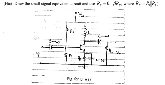
Homework Answers
Request Answer!
We need at least 10 more requests to produce the answer.
0 / 10 have requested this problem solution
The more requests, the faster the answer.
Add Answer to:
Design the inductively coupled common emitter (CE) amplifier
shown in Fig. for Q. 7(a) to drive...
1. Design the common-emitter amplifier in Fig. 4(a) with the following specifications: Supply Vol...
 Figure 4. (a)
1. Design the common-emitter amplifier in Fig. 4(a) with the following specifications: Supply Voltage, Vcc 0-to-Peak Output Swing, V Voltage Gain, A. Input Resistance, R Output Resistance, Ro THD for 5kHz 1 V (0-to-peak) Sine Wave Output Voltage, V Relative Variation of Ic for VBE 0.7t 0.1V Transistor's Current Gain, β 5V 25 1.8kS2 4% 10% 100 Show your design procedure and all your calculations. Your design should be insensitive to B variations. Vcc RB1 Rc 0...
Figure 4. (a)
1. Design the common-emitter amplifier in Fig. 4(a) with the following specifications: Supply Voltage, Vcc 0-to-Peak Output Swing, V Voltage Gain, A. Input Resistance, R Output Resistance, Ro THD for 5kHz 1 V (0-to-peak) Sine Wave Output Voltage, V Relative Variation of Ic for VBE 0.7t 0.1V Transistor's Current Gain, β 5V 25 1.8kS2 4% 10% 100 Show your design procedure and all your calculations. Your design should be insensitive to B variations. Vcc RB1 Rc 0...
Design a BJT amplifier based on the specifications provided in the table below. Your design shoul...
 THE STEPS TO DO SO:
Design a BJT amplifier based on the specifications provided in the table below. Your design should be insensitive to β variations, and both the input and the output should be AC coupled as in Fig. 1. Supply Voltage, Vcc Load Resistance, RL Transistor's Current Gain, β Relative Variation of lc for VBE-0.7 ± 0.1 V 0-to-Peak Output Swing, Vo Voltage Gain, A Input Resistance, R THD for 5kHz IV (0-to-peak) Sine Wave Output Voltage, V。S5%...
THE STEPS TO DO SO:
Design a BJT amplifier based on the specifications provided in the table below. Your design should be insensitive to β variations, and both the input and the output should be AC coupled as in Fig. 1. Supply Voltage, Vcc Load Resistance, RL Transistor's Current Gain, β Relative Variation of lc for VBE-0.7 ± 0.1 V 0-to-Peak Output Swing, Vo Voltage Gain, A Input Resistance, R THD for 5kHz IV (0-to-peak) Sine Wave Output Voltage, V。S5%...
And a load resistor are connected to the common-emitter amplifier in Q2 as A voltage source shown...
 and a load resistor are connected to the common-emitter amplifier in Q2 as A voltage source shown in 02. (Extra om in the following figure. Determine R, Ro, Avoe and A, by making full use of the results of t10Marks) if ν,-20mVpp, determine the output voltage, vo. +10V0V Rep-225 Ci 1002 + R: 5.5k2 Rg 300Ω CE
and a load resistor are connected to the common-emitter amplifier in Q2 as A voltage source shown in 02. (Extra om in the...
and a load resistor are connected to the common-emitter amplifier in Q2 as A voltage source shown in 02. (Extra om in the following figure. Determine R, Ro, Avoe and A, by making full use of the results of t10Marks) if ν,-20mVpp, determine the output voltage, vo. +10V0V Rep-225 Ci 1002 + R: 5.5k2 Rg 300Ω CE
and a load resistor are connected to the common-emitter amplifier in Q2 as A voltage source shown in 02. (Extra om in the...
Perform a simple initial design of an ac coupled common-emitter amplifier with four resistor biasing and emitter by-pass...
 Perform a simple initial design of an ac coupled common-emitter
amplifier with
four resistor biasing and emitter by-pass capacitor, to have a
voltage gain of about
100, for the following conditions. Justify any approximations used.
(Assume Ic=1/300 A)
i)Transistor ac common-emitter gain, B, 100 ii) Supply voltage ofV0c-20V iii) Allow 10% Vcc across RE DC collector voltage of 10 V iv) v) DC current in the base bias resistors should be ten times greater than the DC base current. Assume...
Perform a simple initial design of an ac coupled common-emitter
amplifier with
four resistor biasing and emitter by-pass capacitor, to have a
voltage gain of about
100, for the following conditions. Justify any approximations used.
(Assume Ic=1/300 A)
i)Transistor ac common-emitter gain, B, 100 ii) Supply voltage ofV0c-20V iii) Allow 10% Vcc across RE DC collector voltage of 10 V iv) v) DC current in the base bias resistors should be ten times greater than the DC base current. Assume...
6.5 BI C2 Cl sig in 0 Design the bias circuit of the CE amplifier shown...
 6.5 BI C2 Cl sig in 0 Design the bias circuit of the CE amplifier shown to obtain IE= 0.5 mA and Vc= +6 V. Design for a dc voltage at the base of 5 V and a current through RB2 of 50 μΑ. Let Vcc-+15 V, β-100, and VBE 0.7 V. a) Specify the values of RBi, RB2, RE, and Rc b) Also give the values of the BJT small-signal parameters gm, rr , and ro at the bias...
4. Consider the BJT cascade amplifier shown below Vcc 18V R1 3.3ko 15uF r Vo RL...
 4. Consider the BJT cascade amplifier shown below Vcc 18V R1 3.3ko 15uF r Vo RL B 150 Rsa 500? 56k? Vi B 150 C1 CE 2.2k? a) Find the DC collector current (approximately the same in both transistors). b) Find the input impedance, output impedance, and no-load voltage gain. c) Find the Av, Avs, and Ai d) Estimate the lower cutoff frequency e) Why does this amplifier have better high-frequency performance thana common-emitter built using the same type of...
please I need details l and....Debate Club | Offic A) Theoretical Design Design a common emitter BJT amplifier with the following requirements: -Rin-10 K2, and Ro-45 ㏀ (Neglect the Early voltage...
 please I need details
l and....Debate Club | Offic A) Theoretical Design Design a common emitter BJT amplifier with the following requirements: -Rin-10 K2, and Ro-45 ㏀ (Neglect the Early voltage Effect) Vo/Vsig- Gv-40 VIV or 32 dB " VCC-9 V V, IC-1mA, VCE-3.25V and β-100 RL-40 kQ, Rsige I ka, R 1-3R2, and C1-C2-1 μF Voc RC C2 R1 Rsig C1 RL R2 RE B) Verify your design using Orcad Capture Pspice by doing 1) AC sweep (frequency response):...
please I need details
l and....Debate Club | Offic A) Theoretical Design Design a common emitter BJT amplifier with the following requirements: -Rin-10 K2, and Ro-45 ㏀ (Neglect the Early voltage Effect) Vo/Vsig- Gv-40 VIV or 32 dB " VCC-9 V V, IC-1mA, VCE-3.25V and β-100 RL-40 kQ, Rsige I ka, R 1-3R2, and C1-C2-1 μF Voc RC C2 R1 Rsig C1 RL R2 RE B) Verify your design using Orcad Capture Pspice by doing 1) AC sweep (frequency response):...
Q.A. 2 -Statement: DC biasing of a CE amplifier circuit is as in Fig.2 Assume the...
 Q.A. 2 -Statement: DC biasing of a CE amplifier
circuit is as in Fig.2 Assume the parameters, VCC
= 12 volt, RE = 450 ohm; = 100; RL = 2250 ohm, RC =1000 ohm and
source resistance and Rs = 2500 ohm. Also, the device emitter
resistance re is negligible.
The amplifier is excited by a source, vs(t) = Vm × sin(2ft)
with Vm = 500 mV peak and f = 5500 Hz; and, coupling and by-pass
capacitors can...
Q.A. 2 -Statement: DC biasing of a CE amplifier
circuit is as in Fig.2 Assume the parameters, VCC
= 12 volt, RE = 450 ohm; = 100; RL = 2250 ohm, RC =1000 ohm and
source resistance and Rs = 2500 ohm. Also, the device emitter
resistance re is negligible.
The amplifier is excited by a source, vs(t) = Vm × sin(2ft)
with Vm = 500 mV peak and f = 5500 Hz; and, coupling and by-pass
capacitors can...
A common-emitter BJT amplificr is shown in Fig.8.1. Note the DC biasing values and the BJTsmall-s...
 A common-emitter BJT amplificr is shown in Fig.8.1. Note the DC biasing values and the BJTsmall-signalmodel parameters from the class-signment #9 on DC Bia ing. Neglect the value of Rs in your calculations, k1 Rs-a k2: 1· Cal ulatethesmall-agalpannetas ofthe amplifi randcompletethecalculated valuesinTable8-1 Smalls-signal voltage gai, AVk Small-signal input resistance,k, Small-signaloutput resistance, Ro VW RC 2k C2 RB 570k Rs C1 1 10uP 0.1m 1 Vs CE RE 2k SINE(0 1mV 1kHz 0 0 00) tran 0 2ms 0 1us...
can you do 4.83 Ar- Q Sea 100 V, what does the gain become? age at...
 can
you do 4.83
Ar- Q Sea 100 V, what does the gain become? age at the collector. (b) Replacing the transistor by its T model, da the small-signal equivalent circuit of the a plifier. Analyze the resulting circuit to dete mine the voltage gain t/ 04.81 Consider the CE amplifier circuit of Fig. 4.43(a). It is required to design the circuit (i.e., find values for I and Rc) to meet the following specifications: (a) R,5kn (b) the voltage gain...
can
you do 4.83
Ar- Q Sea 100 V, what does the gain become? age at the collector. (b) Replacing the transistor by its T model, da the small-signal equivalent circuit of the a plifier. Analyze the resulting circuit to dete mine the voltage gain t/ 04.81 Consider the CE amplifier circuit of Fig. 4.43(a). It is required to design the circuit (i.e., find values for I and Rc) to meet the following specifications: (a) R,5kn (b) the voltage gain...
 Figure 4. (a)
1. Design the common-emitter amplifier in Fig. 4(a) with the following specifications: Supply Voltage, Vcc 0-to-Peak Output Swing, V Voltage Gain, A. Input Resistance, R Output Resistance, Ro THD for 5kHz 1 V (0-to-peak) Sine Wave Output Voltage, V Relative Variation of Ic for VBE 0.7t 0.1V Transistor's Current Gain, β 5V 25 1.8kS2 4% 10% 100 Show your design procedure and all your calculations. Your design should be insensitive to B variations. Vcc RB1 Rc 0...
Figure 4. (a)
1. Design the common-emitter amplifier in Fig. 4(a) with the following specifications: Supply Voltage, Vcc 0-to-Peak Output Swing, V Voltage Gain, A. Input Resistance, R Output Resistance, Ro THD for 5kHz 1 V (0-to-peak) Sine Wave Output Voltage, V Relative Variation of Ic for VBE 0.7t 0.1V Transistor's Current Gain, β 5V 25 1.8kS2 4% 10% 100 Show your design procedure and all your calculations. Your design should be insensitive to B variations. Vcc RB1 Rc 0...
 THE STEPS TO DO SO:
Design a BJT amplifier based on the specifications provided in the table below. Your design should be insensitive to β variations, and both the input and the output should be AC coupled as in Fig. 1. Supply Voltage, Vcc Load Resistance, RL Transistor's Current Gain, β Relative Variation of lc for VBE-0.7 ± 0.1 V 0-to-Peak Output Swing, Vo Voltage Gain, A Input Resistance, R THD for 5kHz IV (0-to-peak) Sine Wave Output Voltage, V。S5%...
THE STEPS TO DO SO:
Design a BJT amplifier based on the specifications provided in the table below. Your design should be insensitive to β variations, and both the input and the output should be AC coupled as in Fig. 1. Supply Voltage, Vcc Load Resistance, RL Transistor's Current Gain, β Relative Variation of lc for VBE-0.7 ± 0.1 V 0-to-Peak Output Swing, Vo Voltage Gain, A Input Resistance, R THD for 5kHz IV (0-to-peak) Sine Wave Output Voltage, V。S5%...
 and a load resistor are connected to the common-emitter amplifier in Q2 as A voltage source shown in 02. (Extra om in the following figure. Determine R, Ro, Avoe and A, by making full use of the results of t10Marks) if ν,-20mVpp, determine the output voltage, vo. +10V0V Rep-225 Ci 1002 + R: 5.5k2 Rg 300Ω CE
and a load resistor are connected to the common-emitter amplifier in Q2 as A voltage source shown in 02. (Extra om in the...
and a load resistor are connected to the common-emitter amplifier in Q2 as A voltage source shown in 02. (Extra om in the following figure. Determine R, Ro, Avoe and A, by making full use of the results of t10Marks) if ν,-20mVpp, determine the output voltage, vo. +10V0V Rep-225 Ci 1002 + R: 5.5k2 Rg 300Ω CE
and a load resistor are connected to the common-emitter amplifier in Q2 as A voltage source shown in 02. (Extra om in the...
 Perform a simple initial design of an ac coupled common-emitter
amplifier with
four resistor biasing and emitter by-pass capacitor, to have a
voltage gain of about
100, for the following conditions. Justify any approximations used.
(Assume Ic=1/300 A)
i)Transistor ac common-emitter gain, B, 100 ii) Supply voltage ofV0c-20V iii) Allow 10% Vcc across RE DC collector voltage of 10 V iv) v) DC current in the base bias resistors should be ten times greater than the DC base current. Assume...
Perform a simple initial design of an ac coupled common-emitter
amplifier with
four resistor biasing and emitter by-pass capacitor, to have a
voltage gain of about
100, for the following conditions. Justify any approximations used.
(Assume Ic=1/300 A)
i)Transistor ac common-emitter gain, B, 100 ii) Supply voltage ofV0c-20V iii) Allow 10% Vcc across RE DC collector voltage of 10 V iv) v) DC current in the base bias resistors should be ten times greater than the DC base current. Assume...
 6.5 BI C2 Cl sig in 0 Design the bias circuit of the CE amplifier shown to obtain IE= 0.5 mA and Vc= +6 V. Design for a dc voltage at the base of 5 V and a current through RB2 of 50 μΑ. Let Vcc-+15 V, β-100, and VBE 0.7 V. a) Specify the values of RBi, RB2, RE, and Rc b) Also give the values of the BJT small-signal parameters gm, rr , and ro at the bias...
 4. Consider the BJT cascade amplifier shown below Vcc 18V R1 3.3ko 15uF r Vo RL B 150 Rsa 500? 56k? Vi B 150 C1 CE 2.2k? a) Find the DC collector current (approximately the same in both transistors). b) Find the input impedance, output impedance, and no-load voltage gain. c) Find the Av, Avs, and Ai d) Estimate the lower cutoff frequency e) Why does this amplifier have better high-frequency performance thana common-emitter built using the same type of...
 please I need details
l and....Debate Club | Offic A) Theoretical Design Design a common emitter BJT amplifier with the following requirements: -Rin-10 K2, and Ro-45 ㏀ (Neglect the Early voltage Effect) Vo/Vsig- Gv-40 VIV or 32 dB " VCC-9 V V, IC-1mA, VCE-3.25V and β-100 RL-40 kQ, Rsige I ka, R 1-3R2, and C1-C2-1 μF Voc RC C2 R1 Rsig C1 RL R2 RE B) Verify your design using Orcad Capture Pspice by doing 1) AC sweep (frequency response):...
please I need details
l and....Debate Club | Offic A) Theoretical Design Design a common emitter BJT amplifier with the following requirements: -Rin-10 K2, and Ro-45 ㏀ (Neglect the Early voltage Effect) Vo/Vsig- Gv-40 VIV or 32 dB " VCC-9 V V, IC-1mA, VCE-3.25V and β-100 RL-40 kQ, Rsige I ka, R 1-3R2, and C1-C2-1 μF Voc RC C2 R1 Rsig C1 RL R2 RE B) Verify your design using Orcad Capture Pspice by doing 1) AC sweep (frequency response):...
 Q.A. 2 -Statement: DC biasing of a CE amplifier
circuit is as in Fig.2 Assume the parameters, VCC
= 12 volt, RE = 450 ohm; = 100; RL = 2250 ohm, RC =1000 ohm and
source resistance and Rs = 2500 ohm. Also, the device emitter
resistance re is negligible.
The amplifier is excited by a source, vs(t) = Vm × sin(2ft)
with Vm = 500 mV peak and f = 5500 Hz; and, coupling and by-pass
capacitors can...
Q.A. 2 -Statement: DC biasing of a CE amplifier
circuit is as in Fig.2 Assume the parameters, VCC
= 12 volt, RE = 450 ohm; = 100; RL = 2250 ohm, RC =1000 ohm and
source resistance and Rs = 2500 ohm. Also, the device emitter
resistance re is negligible.
The amplifier is excited by a source, vs(t) = Vm × sin(2ft)
with Vm = 500 mV peak and f = 5500 Hz; and, coupling and by-pass
capacitors can...
 A common-emitter BJT amplificr is shown in Fig.8.1. Note the DC biasing values and the BJTsmall-signalmodel parameters from the class-signment #9 on DC Bia ing. Neglect the value of Rs in your calculations, k1 Rs-a k2: 1· Cal ulatethesmall-agalpannetas ofthe amplifi randcompletethecalculated valuesinTable8-1 Smalls-signal voltage gai, AVk Small-signal input resistance,k, Small-signaloutput resistance, Ro VW RC 2k C2 RB 570k Rs C1 1 10uP 0.1m 1 Vs CE RE 2k SINE(0 1mV 1kHz 0 0 00) tran 0 2ms 0 1us...
 can
you do 4.83
Ar- Q Sea 100 V, what does the gain become? age at the collector. (b) Replacing the transistor by its T model, da the small-signal equivalent circuit of the a plifier. Analyze the resulting circuit to dete mine the voltage gain t/ 04.81 Consider the CE amplifier circuit of Fig. 4.43(a). It is required to design the circuit (i.e., find values for I and Rc) to meet the following specifications: (a) R,5kn (b) the voltage gain...
can
you do 4.83
Ar- Q Sea 100 V, what does the gain become? age at the collector. (b) Replacing the transistor by its T model, da the small-signal equivalent circuit of the a plifier. Analyze the resulting circuit to dete mine the voltage gain t/ 04.81 Consider the CE amplifier circuit of Fig. 4.43(a). It is required to design the circuit (i.e., find values for I and Rc) to meet the following specifications: (a) R,5kn (b) the voltage gain...
Most questions answered within 3 hours.
-
if a firm producing 100 units at $5.00 each experience
an 80% experience curve, what will...
asked 25 minutes ago -
A solid, uniform disk of radius 0.250 m and mass 53.7 kg rolls
down a ramp...
asked 2 hours ago -
Given the following table of high speed internet access vs.
annual home income:
Home Income
%...
asked 3 hours ago -
A baseball batter hits a 0.145kg baseball straight up into the
air. The baseball leaves the...
asked 3 hours ago -
An FM modulator is tested using
single-tone baseband signal with frequency of 50kHz and a sprectrum...
asked 4 hours ago -
Write the ionic equations for the first stage of salts
hydrolysis.
Anion, Cation?
Na2S
NiSO4
K2SO4...
asked 5 hours ago -
suppose there is a normally distributed population with a mean of
250 and a standard deviation...
asked 6 hours ago -
Question Three
Suppose you as project manager are using the Waterfall
development methodology on a large...
asked 7 hours ago -
Which statement is not true about welfare in Canada?
A.Benefits typically vary based on one's ability...
asked 7 hours ago -
Please help me with FLOWCHART and UML diagram for class,
thank you!
#include <iostream>
#include <fstream>...
asked 8 hours ago -
3. Describe the “logic circuit” of the Lac operon. Which
proteins are bound or not to...
asked 8 hours ago -
Ayesha’s adjusted gross income is $60,000 in 2019. She donated a
piece of artwork with a...
asked 8 hours ago