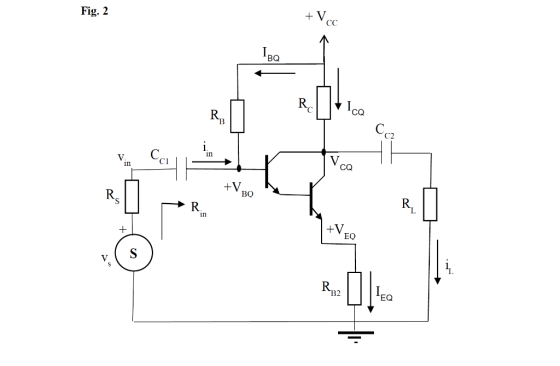
Q.A. 2 -Statement: DC biasing of a CE amplifier circuit is as in Fig.2 Assume the parameters, VCC = 12 volt, RE = 450 ohm; = 100; RL = 2250 ohm, RC =1000 ohm and source resistance and Rs = 2500 ohm. Also, the device emitter resistance re is negligible.
The amplifier is excited by a source, vs(t) = Vm × sin(2ft) with Vm = 500 mV peak and f = 5500 Hz; and, coupling and by-pass capacitors can be assumed to be of zero reactance at the working frequency.
Required Solutions: Determine the following: Input resistance Rin (as seen by the ac signal source at the input); value of biasing resistance, RB, ac power dissipated (PL) in the load, RL and quiescent parameters: (VCQ; ICQ; IBQ; IEQ).
Multiple-choice answers
1. (Rin ≈ 6.61 Mohm; RB ≈ 7.1 Mohm; quiescent parameters: (VCQ ≈ 10.1 volt; ICQ= 3.9 mA; IBQ = 0.45 microA; IEQ = 6.91 mA; and, PL (microwatts) = 100.4)
2. (Rin ≈ 5.42 Mohm; RB ≈ 37.8 Mohm; quiescent parameters: (VCQ ≈ 10.7 volt; ICQ= 4.65 mA; IBQ = 0.23 microA; IEQ = 3.72 mA; and, PL (microwatts) = 80.5)
3. (Rin ≈ 4.55 Mohm; RB ≈ 67.8 Mohm; quiescent parameters: (VCQ ≈ 10.7 volt; ICQ= 3.65 mA; IBQ = 0.33 microA; IEQ = 4.02 mA; and, PL (microwatts) = 102.5)
4. (Rin ≈ 4.42 Mohm; RB ≈ 57.8 Mohm; quiescent parameters: (VCQ ≈ 9.7 volt; ICQ= 5.65 mA; IBQ = 0.30 microA; IEQ = 4.74 mA; and, PL (microwatts) = 69.2)
5. (Rin ≈ 3.61 Mohm; RB ≈ 17.1 Mohm; quiescent parameters: (VCQ ≈ 7.1 volt; ICQ= 4.9 mA; IBQ = 0.49 microA; IEQ = 4.94 mA; and, PL (microwatts) = 113.4)
Homework Answers


Add Answer to:
Q.A. 2 -Statement: DC biasing of a CE amplifier
circuit is as in Fig.2 Assume the...
ASAP! Please answer this question showing steps for thumb up! Question 1 (4 Marks) Q.A. 1...
 ASAP! Please answer this question showing steps for
thumb up!
Question 1 (4 Marks) Q.A. 1 -Statement: DC biasing of a CE amplifier circuit is as in Fig. Q.1. Assume the parameters, Vcc = 18 volt, RE = 500 ohm; B = 125; RL = 1000 ohm, Rc =1500 ohm and source resistance and Rs 1500 ohm. The amplifier is excited by a source, vs(t) = Vm * sin(2teft) with Vm = 25 mV peak and f = 1000 Hz;...
ASAP! Please answer this question showing steps for
thumb up!
Question 1 (4 Marks) Q.A. 1 -Statement: DC biasing of a CE amplifier circuit is as in Fig. Q.1. Assume the parameters, Vcc = 18 volt, RE = 500 ohm; B = 125; RL = 1000 ohm, Rc =1500 ohm and source resistance and Rs 1500 ohm. The amplifier is excited by a source, vs(t) = Vm * sin(2teft) with Vm = 25 mV peak and f = 1000 Hz;...
please pick one of the multiple choice options above. show all work, thank you Question 9...
 please pick one of the multiple choice options above.
show all work, thank you
Question 9 CIRCUIT X/FIG.9 (5 Marks) Statement: Consider the RC-coupled amplifier circuit illustrated in Fig. 9 (CIRCUIT X). Sketching relevant output (Vc-Ic) characteristics that decide Q-point coordinates and DC load-line details (of the NPN-BJT/Si circuit of Fig. 9 of Circuit X) Further, establish an appropriate AC-load line and decide the maximum swing of the output voltage across Rload with respect to the Q-point. Assume the input...
please pick one of the multiple choice options above.
show all work, thank you
Question 9 CIRCUIT X/FIG.9 (5 Marks) Statement: Consider the RC-coupled amplifier circuit illustrated in Fig. 9 (CIRCUIT X). Sketching relevant output (Vc-Ic) characteristics that decide Q-point coordinates and DC load-line details (of the NPN-BJT/Si circuit of Fig. 9 of Circuit X) Further, establish an appropriate AC-load line and decide the maximum swing of the output voltage across Rload with respect to the Q-point. Assume the input...
choose one of the multiple choice answers above. please show all work Question: 10 CIRCUIT Y...
 choose one of the multiple choice answers above.
please show all work
Question: 10 CIRCUIT Y FIG.10 (5 Marks) Statement: Consider the RC-coupled amplifier circuit illustrated in Fig. 10 (CIRCUIT Y). Sketching relevant output (Vc-Ic) characteristics, decide Q-point coordinates and DC load-line details (of the NPN-BJT/Si circuit of Fig. 10 of Circuit Y). Further, establish an appropriate AC-load line and decide the maximum swing of the output voltage across Rload with respect to the Q-point. Assume the input signal at...
choose one of the multiple choice answers above.
please show all work
Question: 10 CIRCUIT Y FIG.10 (5 Marks) Statement: Consider the RC-coupled amplifier circuit illustrated in Fig. 10 (CIRCUIT Y). Sketching relevant output (Vc-Ic) characteristics, decide Q-point coordinates and DC load-line details (of the NPN-BJT/Si circuit of Fig. 10 of Circuit Y). Further, establish an appropriate AC-load line and decide the maximum swing of the output voltage across Rload with respect to the Q-point. Assume the input signal at...
Problem 2: BJT Small-Signal Voltage Amplifiers in the lectures, we covered in detail the analysis of an npn BJT amplifier that utilizes a single-supply DC biasing. In this problem, you will meet...
 Problem 2: BJT Small-Signal Voltage Amplifiers in the lectures, we covered in detail the analysis of an npn BJT amplifier that utilizes a single-supply DC biasing. In this problem, you will meet two additional amplifier architectures- one that is based on dual DC supplies combined with a DC current source, and the other that utilizes a pnp BJT with single-supply biasing. In both problems (below) you need to manually find the amplifier's Q-point (that is, the DC values of Ic...
Electronics1. It's a multiple choices question. use the formula sheet if needed (the last picture). Question...
 Electronics1. It's a multiple choices question. use the formula
sheet if needed (the last picture).
Question 9 CIRCUIT X/FIG.9 (5 Marks) Statement: Consider the RC-coupled amplifier circuit illustrated in Fig. 9 (CIRCUIT X). Sketching relevant output (V-I) characteristics that decide Q-point coordinates and DC load-line details of the NPN-BJT/Si circuit of Fig. 9 of Circuit x) Further, establish an appropriate AC-load line and decide the maximum swing of the output voltage across Road with respect to the Q-point. Assume the...
Electronics1. It's a multiple choices question. use the formula
sheet if needed (the last picture).
Question 9 CIRCUIT X/FIG.9 (5 Marks) Statement: Consider the RC-coupled amplifier circuit illustrated in Fig. 9 (CIRCUIT X). Sketching relevant output (V-I) characteristics that decide Q-point coordinates and DC load-line details of the NPN-BJT/Si circuit of Fig. 9 of Circuit x) Further, establish an appropriate AC-load line and decide the maximum swing of the output voltage across Road with respect to the Q-point. Assume the...
Electronics1. It's a multiple choices question. use the formula sheet if needed (the last picture). Statement:...
 Electronics1. It's a multiple choices question. use the formula
sheet if needed (the last picture).
Statement: Sketching relevant output (Vel) characteristics decide on Q-point coordinates and DC load-line details: That is, determine DC operating conditions of the NPN-BJT/Si circuit of Fig.8 (denoting the type Circuit D2). Assume the following: Vec= 10 volt; V: - 1.8 volt; Re-2.0 k; Re-25 k and a -0.98958. Voc RC Rai Vc V Rusy RE 1 FIG.8: CIRCUIT D2 Required Solutions In the multiple choice...
Electronics1. It's a multiple choices question. use the formula
sheet if needed (the last picture).
Statement: Sketching relevant output (Vel) characteristics decide on Q-point coordinates and DC load-line details: That is, determine DC operating conditions of the NPN-BJT/Si circuit of Fig.8 (denoting the type Circuit D2). Assume the following: Vec= 10 volt; V: - 1.8 volt; Re-2.0 k; Re-25 k and a -0.98958. Voc RC Rai Vc V Rusy RE 1 FIG.8: CIRCUIT D2 Required Solutions In the multiple choice...
Problem 2: BJT Small-Signal Voltage Amplifiers In the lectures, we covered in detail the analysis...
 Problem 2: BJT Small-Signal Voltage Amplifiers In the lectures, we covered in detail the analysis of an npn BJT amplifier that utilizes a single-supply DC biasing. In this problem, you wi meet two additional amplifier architectures-one that is based on dual DC supplies combined with a DC current source, and the other that utilizes a pnp BJT with single-supply biasing In both problems (below) you need to manually find the amplifier's Q-point (that is, the DC values of Ic and...
Electronics1. It's a multiple choices question. use the formula sheet if needed (the last picture). Statement:...
 Electronics1. It's a multiple choices question. use the formula
sheet if needed (the last picture).
Statement: Sketching relevant output (Vele) characteristics decide on Q-point coordinates and DC load-line details: That is, determine DC operating conditions of the NPN-BJT/Si circuit of Fig. 7 (denoting the type Circuit C2). Assume the following: Voc = 18 volt; Ve=0.7; R = 1.5 k: Re2 = 33 k; Vc = 9.5 volt; Inc = 9.5 and, B = 100 Voc Re lac Ro Ne I...
Electronics1. It's a multiple choices question. use the formula
sheet if needed (the last picture).
Statement: Sketching relevant output (Vele) characteristics decide on Q-point coordinates and DC load-line details: That is, determine DC operating conditions of the NPN-BJT/Si circuit of Fig. 7 (denoting the type Circuit C2). Assume the following: Voc = 18 volt; Ve=0.7; R = 1.5 k: Re2 = 33 k; Vc = 9.5 volt; Inc = 9.5 and, B = 100 Voc Re lac Ro Ne I...
Electronics1. It's a multiple choices question. use the formula sheet if needed (the last picture). Question...
 Electronics1. It's a multiple choices question. use the formula
sheet if needed (the last picture).
Question 6 CIRCUIT C2 (2.5 Marks) Statement: Sketching relevant output (Velc) characteristics decide on Q-point coordinates and DC load-line details: That is, determine DC operating conditions of the NPN-BJT/Si circuit of Fig.6 (denoting the type Circuit C2). Assume the following: Vcc= 30 volt; Re-2.0 k; R31 – 15 k; Ra2 = 7.5 k; ; Re-2.0k; V: - 9.3 volt; and, a -0.98684 +Vec Ic Re:...
Electronics1. It's a multiple choices question. use the formula
sheet if needed (the last picture).
Question 6 CIRCUIT C2 (2.5 Marks) Statement: Sketching relevant output (Velc) characteristics decide on Q-point coordinates and DC load-line details: That is, determine DC operating conditions of the NPN-BJT/Si circuit of Fig.6 (denoting the type Circuit C2). Assume the following: Vcc= 30 volt; Re-2.0 k; R31 – 15 k; Ra2 = 7.5 k; ; Re-2.0k; V: - 9.3 volt; and, a -0.98684 +Vec Ic Re:...
Electronics1. It's a multiple choices question. use the formula sheet if needed (the last picture). Question:...
 Electronics1. It's a multiple choices question. use the
formula sheet if needed (the last picture).
Question: 10 CIRCUIT Y/FIG.10 (5 Marks) Statement: Consider the RC-coupled amplifier circuit illustrated in Fig. 10 (CIRCUIT Y). Sketching relevant output (Vc-le) characteristics, decide Q-point coordinates and DC load-line details of the NPN-BJT/Si circuit of Fig.10 of Circuit Y). Further, establish an appropriate AC-load line and decide the maximum swing of the output voltage across Road with respect to the Q-point. Assume the input signal...
Electronics1. It's a multiple choices question. use the
formula sheet if needed (the last picture).
Question: 10 CIRCUIT Y/FIG.10 (5 Marks) Statement: Consider the RC-coupled amplifier circuit illustrated in Fig. 10 (CIRCUIT Y). Sketching relevant output (Vc-le) characteristics, decide Q-point coordinates and DC load-line details of the NPN-BJT/Si circuit of Fig.10 of Circuit Y). Further, establish an appropriate AC-load line and decide the maximum swing of the output voltage across Road with respect to the Q-point. Assume the input signal...
 ASAP! Please answer this question showing steps for
thumb up!
Question 1 (4 Marks) Q.A. 1 -Statement: DC biasing of a CE amplifier circuit is as in Fig. Q.1. Assume the parameters, Vcc = 18 volt, RE = 500 ohm; B = 125; RL = 1000 ohm, Rc =1500 ohm and source resistance and Rs 1500 ohm. The amplifier is excited by a source, vs(t) = Vm * sin(2teft) with Vm = 25 mV peak and f = 1000 Hz;...
ASAP! Please answer this question showing steps for
thumb up!
Question 1 (4 Marks) Q.A. 1 -Statement: DC biasing of a CE amplifier circuit is as in Fig. Q.1. Assume the parameters, Vcc = 18 volt, RE = 500 ohm; B = 125; RL = 1000 ohm, Rc =1500 ohm and source resistance and Rs 1500 ohm. The amplifier is excited by a source, vs(t) = Vm * sin(2teft) with Vm = 25 mV peak and f = 1000 Hz;...
 please pick one of the multiple choice options above.
show all work, thank you
Question 9 CIRCUIT X/FIG.9 (5 Marks) Statement: Consider the RC-coupled amplifier circuit illustrated in Fig. 9 (CIRCUIT X). Sketching relevant output (Vc-Ic) characteristics that decide Q-point coordinates and DC load-line details (of the NPN-BJT/Si circuit of Fig. 9 of Circuit X) Further, establish an appropriate AC-load line and decide the maximum swing of the output voltage across Rload with respect to the Q-point. Assume the input...
please pick one of the multiple choice options above.
show all work, thank you
Question 9 CIRCUIT X/FIG.9 (5 Marks) Statement: Consider the RC-coupled amplifier circuit illustrated in Fig. 9 (CIRCUIT X). Sketching relevant output (Vc-Ic) characteristics that decide Q-point coordinates and DC load-line details (of the NPN-BJT/Si circuit of Fig. 9 of Circuit X) Further, establish an appropriate AC-load line and decide the maximum swing of the output voltage across Rload with respect to the Q-point. Assume the input...
 choose one of the multiple choice answers above.
please show all work
Question: 10 CIRCUIT Y FIG.10 (5 Marks) Statement: Consider the RC-coupled amplifier circuit illustrated in Fig. 10 (CIRCUIT Y). Sketching relevant output (Vc-Ic) characteristics, decide Q-point coordinates and DC load-line details (of the NPN-BJT/Si circuit of Fig. 10 of Circuit Y). Further, establish an appropriate AC-load line and decide the maximum swing of the output voltage across Rload with respect to the Q-point. Assume the input signal at...
choose one of the multiple choice answers above.
please show all work
Question: 10 CIRCUIT Y FIG.10 (5 Marks) Statement: Consider the RC-coupled amplifier circuit illustrated in Fig. 10 (CIRCUIT Y). Sketching relevant output (Vc-Ic) characteristics, decide Q-point coordinates and DC load-line details (of the NPN-BJT/Si circuit of Fig. 10 of Circuit Y). Further, establish an appropriate AC-load line and decide the maximum swing of the output voltage across Rload with respect to the Q-point. Assume the input signal at...
 Problem 2: BJT Small-Signal Voltage Amplifiers in the lectures, we covered in detail the analysis of an npn BJT amplifier that utilizes a single-supply DC biasing. In this problem, you will meet two additional amplifier architectures- one that is based on dual DC supplies combined with a DC current source, and the other that utilizes a pnp BJT with single-supply biasing. In both problems (below) you need to manually find the amplifier's Q-point (that is, the DC values of Ic...
 Electronics1. It's a multiple choices question. use the formula
sheet if needed (the last picture).
Question 9 CIRCUIT X/FIG.9 (5 Marks) Statement: Consider the RC-coupled amplifier circuit illustrated in Fig. 9 (CIRCUIT X). Sketching relevant output (V-I) characteristics that decide Q-point coordinates and DC load-line details of the NPN-BJT/Si circuit of Fig. 9 of Circuit x) Further, establish an appropriate AC-load line and decide the maximum swing of the output voltage across Road with respect to the Q-point. Assume the...
Electronics1. It's a multiple choices question. use the formula
sheet if needed (the last picture).
Question 9 CIRCUIT X/FIG.9 (5 Marks) Statement: Consider the RC-coupled amplifier circuit illustrated in Fig. 9 (CIRCUIT X). Sketching relevant output (V-I) characteristics that decide Q-point coordinates and DC load-line details of the NPN-BJT/Si circuit of Fig. 9 of Circuit x) Further, establish an appropriate AC-load line and decide the maximum swing of the output voltage across Road with respect to the Q-point. Assume the...
 Electronics1. It's a multiple choices question. use the formula
sheet if needed (the last picture).
Statement: Sketching relevant output (Vel) characteristics decide on Q-point coordinates and DC load-line details: That is, determine DC operating conditions of the NPN-BJT/Si circuit of Fig.8 (denoting the type Circuit D2). Assume the following: Vec= 10 volt; V: - 1.8 volt; Re-2.0 k; Re-25 k and a -0.98958. Voc RC Rai Vc V Rusy RE 1 FIG.8: CIRCUIT D2 Required Solutions In the multiple choice...
Electronics1. It's a multiple choices question. use the formula
sheet if needed (the last picture).
Statement: Sketching relevant output (Vel) characteristics decide on Q-point coordinates and DC load-line details: That is, determine DC operating conditions of the NPN-BJT/Si circuit of Fig.8 (denoting the type Circuit D2). Assume the following: Vec= 10 volt; V: - 1.8 volt; Re-2.0 k; Re-25 k and a -0.98958. Voc RC Rai Vc V Rusy RE 1 FIG.8: CIRCUIT D2 Required Solutions In the multiple choice...
 Problem 2: BJT Small-Signal Voltage Amplifiers In the lectures, we covered in detail the analysis of an npn BJT amplifier that utilizes a single-supply DC biasing. In this problem, you wi meet two additional amplifier architectures-one that is based on dual DC supplies combined with a DC current source, and the other that utilizes a pnp BJT with single-supply biasing In both problems (below) you need to manually find the amplifier's Q-point (that is, the DC values of Ic and...
 Electronics1. It's a multiple choices question. use the formula
sheet if needed (the last picture).
Statement: Sketching relevant output (Vele) characteristics decide on Q-point coordinates and DC load-line details: That is, determine DC operating conditions of the NPN-BJT/Si circuit of Fig. 7 (denoting the type Circuit C2). Assume the following: Voc = 18 volt; Ve=0.7; R = 1.5 k: Re2 = 33 k; Vc = 9.5 volt; Inc = 9.5 and, B = 100 Voc Re lac Ro Ne I...
Electronics1. It's a multiple choices question. use the formula
sheet if needed (the last picture).
Statement: Sketching relevant output (Vele) characteristics decide on Q-point coordinates and DC load-line details: That is, determine DC operating conditions of the NPN-BJT/Si circuit of Fig. 7 (denoting the type Circuit C2). Assume the following: Voc = 18 volt; Ve=0.7; R = 1.5 k: Re2 = 33 k; Vc = 9.5 volt; Inc = 9.5 and, B = 100 Voc Re lac Ro Ne I...
 Electronics1. It's a multiple choices question. use the formula
sheet if needed (the last picture).
Question 6 CIRCUIT C2 (2.5 Marks) Statement: Sketching relevant output (Velc) characteristics decide on Q-point coordinates and DC load-line details: That is, determine DC operating conditions of the NPN-BJT/Si circuit of Fig.6 (denoting the type Circuit C2). Assume the following: Vcc= 30 volt; Re-2.0 k; R31 – 15 k; Ra2 = 7.5 k; ; Re-2.0k; V: - 9.3 volt; and, a -0.98684 +Vec Ic Re:...
Electronics1. It's a multiple choices question. use the formula
sheet if needed (the last picture).
Question 6 CIRCUIT C2 (2.5 Marks) Statement: Sketching relevant output (Velc) characteristics decide on Q-point coordinates and DC load-line details: That is, determine DC operating conditions of the NPN-BJT/Si circuit of Fig.6 (denoting the type Circuit C2). Assume the following: Vcc= 30 volt; Re-2.0 k; R31 – 15 k; Ra2 = 7.5 k; ; Re-2.0k; V: - 9.3 volt; and, a -0.98684 +Vec Ic Re:...
 Electronics1. It's a multiple choices question. use the
formula sheet if needed (the last picture).
Question: 10 CIRCUIT Y/FIG.10 (5 Marks) Statement: Consider the RC-coupled amplifier circuit illustrated in Fig. 10 (CIRCUIT Y). Sketching relevant output (Vc-le) characteristics, decide Q-point coordinates and DC load-line details of the NPN-BJT/Si circuit of Fig.10 of Circuit Y). Further, establish an appropriate AC-load line and decide the maximum swing of the output voltage across Road with respect to the Q-point. Assume the input signal...
Electronics1. It's a multiple choices question. use the
formula sheet if needed (the last picture).
Question: 10 CIRCUIT Y/FIG.10 (5 Marks) Statement: Consider the RC-coupled amplifier circuit illustrated in Fig. 10 (CIRCUIT Y). Sketching relevant output (Vc-le) characteristics, decide Q-point coordinates and DC load-line details of the NPN-BJT/Si circuit of Fig.10 of Circuit Y). Further, establish an appropriate AC-load line and decide the maximum swing of the output voltage across Road with respect to the Q-point. Assume the input signal...
Most questions answered within 3 hours.
-
The Problem: The Case of the Harmonizing Vacations
Your CEO is exploring partnering with a European...
asked 45 minutes ago -
A chemical equation is balanced by adding coefficients in front
of some formulas so that the...
asked 44 minutes ago -
From the literature (reference your sources): What are the
lattice parameters of calcite and aragonite? Why...
asked 1 hour ago -
Your system is rejecting the question am asking which is
preceded by a case study. It...
asked 1 hour ago -
3. On January 2, 2000, Larry creates a trust with himself as
trustee. Larry as trustee...
asked 1 hour ago -
A member of the volleyball team spikes the ball. During this
process, she changes the velocity...
asked 1 hour ago -
Are adult gamers less likely to use a gaming console (Xbox,
PlayStation, Wii, etc...) than teen...
asked 2 hours ago -
The University of
Texas recently reported that 43% of college students aged 18-24
would spend their...
asked 2 hours ago -
The length of stay at a specific emergency department in
Phoenix, Arizona, in 2009 had a...
asked 1 hour ago -
. Please give the mechanism for this type of problem. Step by
Step
The toxin that...
asked 1 hour ago -
If you have a 1M stock solution and you want to dilute 1 :10
with water,...
asked 1 hour ago -
In a load instruction, the effective address is obtained by
A) Retriving the address from a...
asked 1 hour ago