
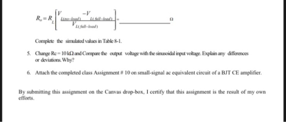
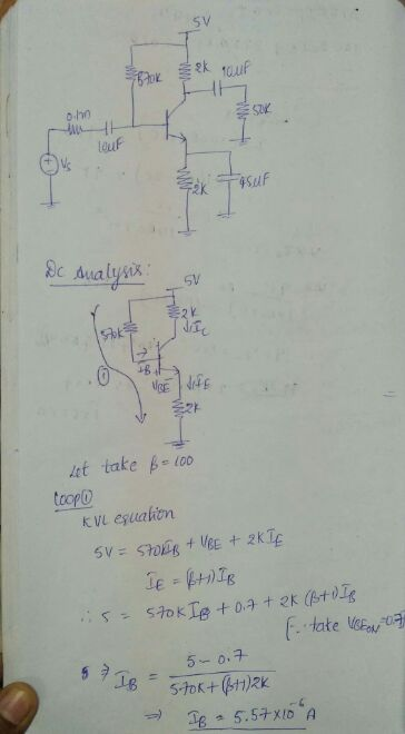
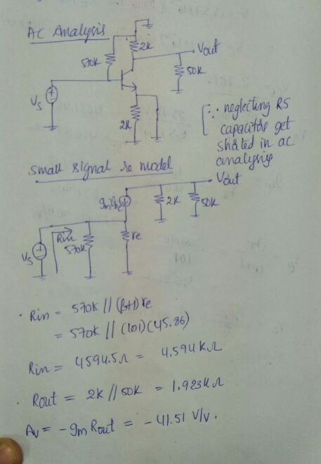
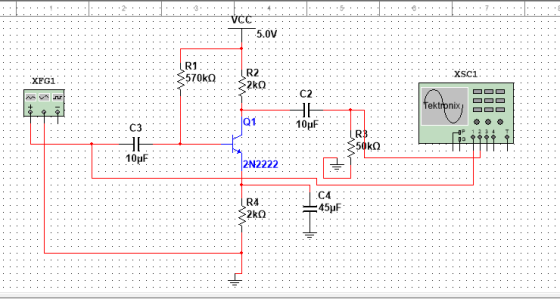
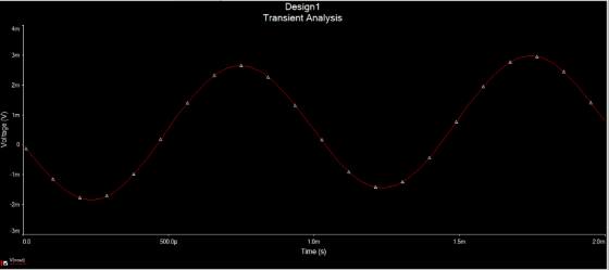
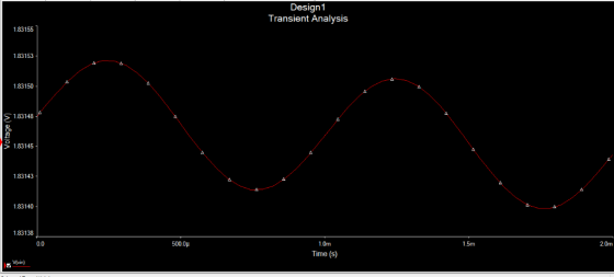
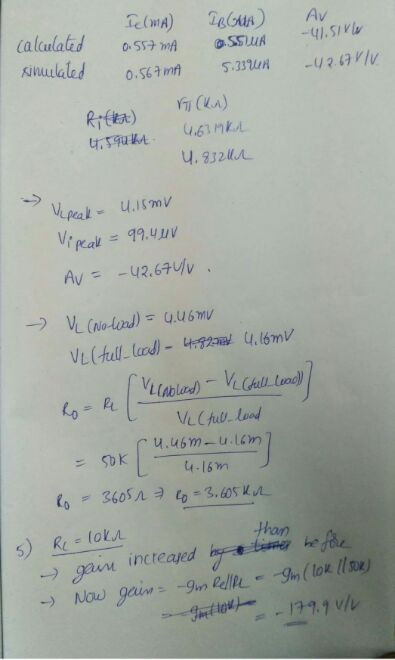
full load Complete the simulated values in Table 8-1 5. Change Rc-10K2 and Compare the output voltage with the sinusoidal input voltage. Explain any differences or deviations. Why? 6. Attach the completed class Assignment #10on small-signal ac equivalent circuit ofa BJT CE amplifier. By submitting this assignment on the Canvas drop-box, I certify that this assignment is the result of my own efforts.
Homework Answers

Add Answer to:
A common-emitter BJT amplificr is shown in Fig.8.1. Note the DC biasing values and the BJTsmall-s...
Problem 2: BJT Small-Signal Voltage Amplifiers in the lectures, we covered in detail the analysis of an npn BJT amplifier that utilizes a single-supply DC biasing. In this problem, you will meet...
 Problem 2: BJT Small-Signal Voltage Amplifiers in the lectures, we covered in detail the analysis of an npn BJT amplifier that utilizes a single-supply DC biasing. In this problem, you will meet two additional amplifier architectures- one that is based on dual DC supplies combined with a DC current source, and the other that utilizes a pnp BJT with single-supply biasing. In both problems (below) you need to manually find the amplifier's Q-point (that is, the DC values of Ic...
i just need help with B, C, D 3) (24 pts) The BJT amplifier shown below....
 i just need help with B, C, D
3) (24 pts) The BJT amplifier shown below. Please answer the following questions. Consider that B=150 VBE=0.75 V and VT-25mV a) What type of amplifier is this? (Select One) CE CE with RE CB b) Find the DC collector current Ic c) Find the transconductance gain gm d) Find the internal small signal voltage gain Au e) Find the input resistance of the small signal amplifier 1) Find the output resistance of...
i just need help with B, C, D
3) (24 pts) The BJT amplifier shown below. Please answer the following questions. Consider that B=150 VBE=0.75 V and VT-25mV a) What type of amplifier is this? (Select One) CE CE with RE CB b) Find the DC collector current Ic c) Find the transconductance gain gm d) Find the internal small signal voltage gain Au e) Find the input resistance of the small signal amplifier 1) Find the output resistance of...
In a small signal voltage amplifier using a pnp transistor shown below, the voltage gain is 350.2. The value of a-0.95. Find the equivalent model emitter resistance re in Ohms if Rc-4.1K2. The BJT is...
 In a small signal voltage amplifier using a pnp transistor shown below, the voltage gain is 350.2. The value of a-0.95. Find the equivalent model emitter resistance re in Ohms if Rc-4.1K2. The BJT is operating at room temperature and VBE 0.7V RE-10K CCI vi Cc2 Rc
In a small signal voltage amplifier using a pnp transistor shown below, the voltage gain is 350.2. The value of a-0.95. Find the equivalent model emitter resistance re in Ohms if Rc-4.1K2. The...
In a small signal voltage amplifier using a pnp transistor shown below, the voltage gain is 350.2. The value of a-0.95. Find the equivalent model emitter resistance re in Ohms if Rc-4.1K2. The BJT is operating at room temperature and VBE 0.7V RE-10K CCI vi Cc2 Rc
In a small signal voltage amplifier using a pnp transistor shown below, the voltage gain is 350.2. The value of a-0.95. Find the equivalent model emitter resistance re in Ohms if Rc-4.1K2. The...
Evaluate the differential input resistance (in kOhms) for a BJT differential amplifier with emitter degeneration resistors of 421.69Ohms, Beta of 66.99, common DC current source of 3.66mA with output...
 Evaluate the differential input resistance (in kOhms) for a BJT differential amplifier with emitter degeneration resistors of 421.69Ohms, Beta of 66.99, common DC current source of 3.66mA with output resistance of 269kOhms. Rct C2 Rs RE le Ro
Evaluate the differential input resistance (in kOhms) for a BJT differential amplifier with emitter degeneration resistors of 421.69Ohms, Beta of 66.99, common DC current source of 3.66mA with output resistance of 269kOhms. Rct C2 Rs RE le Ro
Evaluate the differential input resistance (in kOhms) for a BJT differential amplifier with emitter degeneration resistors of 421.69Ohms, Beta of 66.99, common DC current source of 3.66mA with output resistance of 269kOhms. Rct C2 Rs RE le Ro
FIND THE VALUES OF Rb1, Rb2, Re,Rc, rin , rout, overall gain and open circuit gain First, design a common emitter BJT a...
 FIND THE VALUES OF Rb1, Rb2, Re,Rc, rin , rout, overall gain and
open circuit gain
First, design a common emitter BJT amplifier Second, analyze the amplifier.( Avo, Gv, Rin, Rout) Third, compare your calculation with Multisim. Report must include comparison between your calculation & simulation results overall voltage gain, open circuit voltage gain, input resistance, and output resistance. This design project is not group work, must be done individually. Type your report. Design a discrete common emitter BJT amplifier.(Determine...
FIND THE VALUES OF Rb1, Rb2, Re,Rc, rin , rout, overall gain and
open circuit gain
First, design a common emitter BJT amplifier Second, analyze the amplifier.( Avo, Gv, Rin, Rout) Third, compare your calculation with Multisim. Report must include comparison between your calculation & simulation results overall voltage gain, open circuit voltage gain, input resistance, and output resistance. This design project is not group work, must be done individually. Type your report. Design a discrete common emitter BJT amplifier.(Determine...
QUESTION 2 [Total 20 Marks] Figure 2.1 presents the BJT amplifier's DC biasing voltages (PSpice Biasing...
 QUESTION 2 [Total 20 Marks] Figure 2.1 presents the BJT amplifier's DC biasing voltages (PSpice Biasing Point simulation). In your evaluation assume that ANSWER: the output resistance of the BJT Q1 is infinite a)-29.4x10⁵ A/V Establish the slope of the DC load line Establish the slope of the AC load line Sketch the DC and AC load lines directly on the transistor's Ic vs Vc plot provided in Figure 2.2 a) b) c) [3 marks] 3 marks] b)-75.8x10⁻³ A/ [10...
Q1. For the cascade amplifier circuit shown in Fig (1): a) What are the functions of the capacitors C, C2 and C3? And w...
 Q1. For the cascade amplifier circuit shown in Fig (1): a) What are the functions of the capacitors C, C2 and C3? And what are the functions of the capacitors Cs and CE? b) What are the functions of the resistors RD and Rc? c) Draw the DC biasing circuits for each stage. d) Find loa, VGsa, VDs and gm for the JFET stage (you may use either mathematical or graphical methods) e) Calculate l, Ic, le and Ve for...
3. In Figure 3, the DC operating point for BJT Q, is Ici = 170 uA...
 3. In Figure 3, the DC operating point for BJT Q, is Ici = 170 uA and VCE = 4 V, and the DC operating point for BJT 02 is Ic2 = 240 A and VCE2 = 3 V. Both Q1 and Q2 have B = 100, VA-75 V at the room temperature. Assume that all the capacitors have infinite values, and all the resistors have the values as indicated in Figure 3. (a) (b) Determine the voltage gain 4....
k) Biasing of a BJT transistor is the setting of the collector emitter voltage and the...
 k) Biasing of a BJT transistor is the setting of the collector emitter voltage and the collector current to the desired dc values. These voltages and currents determine the operating point (quiescent point, Q point). The three circuits given in Fig. 6.4 are designed to give the same operating point 12V 12V Rc Rc 12V R1 ?1 Rc R1 ?? Figure 6.4 a. Obtain the expression for VC in terms of the transistor parameters ?, VBE, Ico and the circuit...
1. Design the common-emitter amplifier in Fig. 4(a) with the following specifications: Supply Vol...
 Figure 4. (a)
1. Design the common-emitter amplifier in Fig. 4(a) with the following specifications: Supply Voltage, Vcc 0-to-Peak Output Swing, V Voltage Gain, A. Input Resistance, R Output Resistance, Ro THD for 5kHz 1 V (0-to-peak) Sine Wave Output Voltage, V Relative Variation of Ic for VBE 0.7t 0.1V Transistor's Current Gain, β 5V 25 1.8kS2 4% 10% 100 Show your design procedure and all your calculations. Your design should be insensitive to B variations. Vcc RB1 Rc 0...
Figure 4. (a)
1. Design the common-emitter amplifier in Fig. 4(a) with the following specifications: Supply Voltage, Vcc 0-to-Peak Output Swing, V Voltage Gain, A. Input Resistance, R Output Resistance, Ro THD for 5kHz 1 V (0-to-peak) Sine Wave Output Voltage, V Relative Variation of Ic for VBE 0.7t 0.1V Transistor's Current Gain, β 5V 25 1.8kS2 4% 10% 100 Show your design procedure and all your calculations. Your design should be insensitive to B variations. Vcc RB1 Rc 0...
 Problem 2: BJT Small-Signal Voltage Amplifiers in the lectures, we covered in detail the analysis of an npn BJT amplifier that utilizes a single-supply DC biasing. In this problem, you will meet two additional amplifier architectures- one that is based on dual DC supplies combined with a DC current source, and the other that utilizes a pnp BJT with single-supply biasing. In both problems (below) you need to manually find the amplifier's Q-point (that is, the DC values of Ic...
 i just need help with B, C, D
3) (24 pts) The BJT amplifier shown below. Please answer the following questions. Consider that B=150 VBE=0.75 V and VT-25mV a) What type of amplifier is this? (Select One) CE CE with RE CB b) Find the DC collector current Ic c) Find the transconductance gain gm d) Find the internal small signal voltage gain Au e) Find the input resistance of the small signal amplifier 1) Find the output resistance of...
i just need help with B, C, D
3) (24 pts) The BJT amplifier shown below. Please answer the following questions. Consider that B=150 VBE=0.75 V and VT-25mV a) What type of amplifier is this? (Select One) CE CE with RE CB b) Find the DC collector current Ic c) Find the transconductance gain gm d) Find the internal small signal voltage gain Au e) Find the input resistance of the small signal amplifier 1) Find the output resistance of...
 In a small signal voltage amplifier using a pnp transistor shown below, the voltage gain is 350.2. The value of a-0.95. Find the equivalent model emitter resistance re in Ohms if Rc-4.1K2. The BJT is operating at room temperature and VBE 0.7V RE-10K CCI vi Cc2 Rc
In a small signal voltage amplifier using a pnp transistor shown below, the voltage gain is 350.2. The value of a-0.95. Find the equivalent model emitter resistance re in Ohms if Rc-4.1K2. The...
In a small signal voltage amplifier using a pnp transistor shown below, the voltage gain is 350.2. The value of a-0.95. Find the equivalent model emitter resistance re in Ohms if Rc-4.1K2. The BJT is operating at room temperature and VBE 0.7V RE-10K CCI vi Cc2 Rc
In a small signal voltage amplifier using a pnp transistor shown below, the voltage gain is 350.2. The value of a-0.95. Find the equivalent model emitter resistance re in Ohms if Rc-4.1K2. The...
 Evaluate the differential input resistance (in kOhms) for a BJT differential amplifier with emitter degeneration resistors of 421.69Ohms, Beta of 66.99, common DC current source of 3.66mA with output resistance of 269kOhms. Rct C2 Rs RE le Ro
Evaluate the differential input resistance (in kOhms) for a BJT differential amplifier with emitter degeneration resistors of 421.69Ohms, Beta of 66.99, common DC current source of 3.66mA with output resistance of 269kOhms. Rct C2 Rs RE le Ro
Evaluate the differential input resistance (in kOhms) for a BJT differential amplifier with emitter degeneration resistors of 421.69Ohms, Beta of 66.99, common DC current source of 3.66mA with output resistance of 269kOhms. Rct C2 Rs RE le Ro
 FIND THE VALUES OF Rb1, Rb2, Re,Rc, rin , rout, overall gain and
open circuit gain
First, design a common emitter BJT amplifier Second, analyze the amplifier.( Avo, Gv, Rin, Rout) Third, compare your calculation with Multisim. Report must include comparison between your calculation & simulation results overall voltage gain, open circuit voltage gain, input resistance, and output resistance. This design project is not group work, must be done individually. Type your report. Design a discrete common emitter BJT amplifier.(Determine...
FIND THE VALUES OF Rb1, Rb2, Re,Rc, rin , rout, overall gain and
open circuit gain
First, design a common emitter BJT amplifier Second, analyze the amplifier.( Avo, Gv, Rin, Rout) Third, compare your calculation with Multisim. Report must include comparison between your calculation & simulation results overall voltage gain, open circuit voltage gain, input resistance, and output resistance. This design project is not group work, must be done individually. Type your report. Design a discrete common emitter BJT amplifier.(Determine...
 QUESTION 2 [Total 20 Marks] Figure 2.1 presents the BJT amplifier's DC biasing voltages (PSpice Biasing Point simulation). In your evaluation assume that ANSWER: the output resistance of the BJT Q1 is infinite a)-29.4x10⁵ A/V Establish the slope of the DC load line Establish the slope of the AC load line Sketch the DC and AC load lines directly on the transistor's Ic vs Vc plot provided in Figure 2.2 a) b) c) [3 marks] 3 marks] b)-75.8x10⁻³ A/ [10...
 Q1. For the cascade amplifier circuit shown in Fig (1): a) What are the functions of the capacitors C, C2 and C3? And what are the functions of the capacitors Cs and CE? b) What are the functions of the resistors RD and Rc? c) Draw the DC biasing circuits for each stage. d) Find loa, VGsa, VDs and gm for the JFET stage (you may use either mathematical or graphical methods) e) Calculate l, Ic, le and Ve for...
 3. In Figure 3, the DC operating point for BJT Q, is Ici = 170 uA and VCE = 4 V, and the DC operating point for BJT 02 is Ic2 = 240 A and VCE2 = 3 V. Both Q1 and Q2 have B = 100, VA-75 V at the room temperature. Assume that all the capacitors have infinite values, and all the resistors have the values as indicated in Figure 3. (a) (b) Determine the voltage gain 4....
 k) Biasing of a BJT transistor is the setting of the collector emitter voltage and the collector current to the desired dc values. These voltages and currents determine the operating point (quiescent point, Q point). The three circuits given in Fig. 6.4 are designed to give the same operating point 12V 12V Rc Rc 12V R1 ?1 Rc R1 ?? Figure 6.4 a. Obtain the expression for VC in terms of the transistor parameters ?, VBE, Ico and the circuit...
 Figure 4. (a)
1. Design the common-emitter amplifier in Fig. 4(a) with the following specifications: Supply Voltage, Vcc 0-to-Peak Output Swing, V Voltage Gain, A. Input Resistance, R Output Resistance, Ro THD for 5kHz 1 V (0-to-peak) Sine Wave Output Voltage, V Relative Variation of Ic for VBE 0.7t 0.1V Transistor's Current Gain, β 5V 25 1.8kS2 4% 10% 100 Show your design procedure and all your calculations. Your design should be insensitive to B variations. Vcc RB1 Rc 0...
Figure 4. (a)
1. Design the common-emitter amplifier in Fig. 4(a) with the following specifications: Supply Voltage, Vcc 0-to-Peak Output Swing, V Voltage Gain, A. Input Resistance, R Output Resistance, Ro THD for 5kHz 1 V (0-to-peak) Sine Wave Output Voltage, V Relative Variation of Ic for VBE 0.7t 0.1V Transistor's Current Gain, β 5V 25 1.8kS2 4% 10% 100 Show your design procedure and all your calculations. Your design should be insensitive to B variations. Vcc RB1 Rc 0...
Most questions answered within 3 hours.
-
An MNE is this kind of industry when competition in one country
is essentially independent of...
asked 45 minutes ago -
. For this set of questions, determine what
proportion of a normal distribution is located betweeneach...
asked 1 hour ago -
A college student is employed as a door-to-door newspaper
salesman. Historical data suggests that the student...
asked 2 hours ago -
MATLAB HW 11 problem using Switch Case and Input commands
Write a script file that calculates...
asked 2 hours ago -
Considering gravitational time dilation, calculate the time that
passes in Earth’s surface while 1 hour passes...
asked 2 hours ago -
Minitab Problem: Take the Lake Hume June rainfall data and find
use the processes outlined in...
asked 3 hours ago -
X Company is trying to decide whether to continue using old
equipment to make Product A...
asked 3 hours ago -
IN PYTHON ONLY !! Program 2: Re-work
program #5 (WeeklyHours) from the previous assignment such that...
asked 4 hours ago -
The average length of time between arrivals at a turnpike
toll-booth is 26 seconds. What is...
asked 5 hours ago -
(a) A piston at 6.1 atm contains a gas that occupies a volume of
3.5 L....
asked 7 hours ago -
Please answer true or false. Words
cannot be changed or added in to make it true...
asked 6 hours ago -
An empty test tube weighs 15.923 grams. Then,
MgCl2•6H2O is added into the test tube. After...
asked 7 hours ago