Fundamentals of Electronic Engineering

Answer should be step by step and readable (clear handwriting)
Homework Answers


Add Answer to:
Fundamentals of Electronic Engineering
Answer should be step by step and readable (clear
handwriting)
Given: •...
If you remove the capacitor CE from across Rg in the Common Emitter amplifier, what should...
 If you remove the capacitor CE from across Rg in the Common Emitter amplifier, what should you expected to happen? R1 C2 out C1 01 2N3904 Vin RL R2 CE RE In a Common Emitter amplifier, which components will most significantly impact the Mid-band voltage gain (Av)? Rc R1 C2 out C1 01 2N3904 Vin RL R2 CE RE
1) Calculate the ac emitter resistance r'e for the value of IE = 5.52 mA. (In...
 1) Calculate the ac emitter resistance r'e
for the value of IE = 5.52 mA. (In Ω)
2) Calculate the value of ac load resistance
rL. (In kΩ)
3) Calculate the voltage gain AV.
4) Calculate the value of output voltage.
(Vp-p)
Required information In the circuit below: Vin = 10 mVp-p, R2 = 2.2 k12, R1 = 15 k12, Vcc = 21 V, RC = 3 k12, B = 100, RE = 3602, and RL = 6.2 k12. V...
1) Calculate the ac emitter resistance r'e
for the value of IE = 5.52 mA. (In Ω)
2) Calculate the value of ac load resistance
rL. (In kΩ)
3) Calculate the voltage gain AV.
4) Calculate the value of output voltage.
(Vp-p)
Required information In the circuit below: Vin = 10 mVp-p, R2 = 2.2 k12, R1 = 15 k12, Vcc = 21 V, RC = 3 k12, B = 100, RE = 3602, and RL = 6.2 k12. V...
Assume DC bias current through the resister in parallel with the DC bias current source is...
 Assume DC bias current through the resister in parallel with
the DC bias current source is negligible.
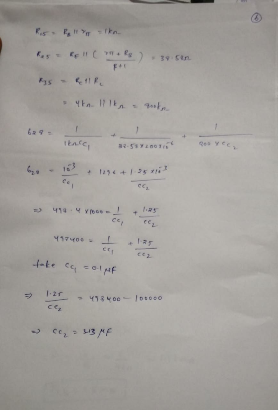
Vcc = 15V R1 100k RC 800 C2 1E-5 Rsig C1 100 1E-5 R2 50k RE 400 Vin 4k Note: This circuit is the same common emitter circuit seen in HW18 and HW19 The internal capacitances are CBE = CBCT 10-12 F. You can assume that CCE is zero. a) Approximately, determine the poles associated with each internal capacitor. Use the Miller Theorem...
Assume DC bias current through the resister in parallel with
the DC bias current source is negligible.
Vcc = 15V R1 100k RC 800 C2 1E-5 Rsig C1 100 1E-5 R2 50k RE 400 Vin 4k Note: This circuit is the same common emitter circuit seen in HW18 and HW19 The internal capacitances are CBE = CBCT 10-12 F. You can assume that CCE is zero. a) Approximately, determine the poles associated with each internal capacitor. Use the Miller Theorem...
Do not answer it , if you do not know how to use pspice
 do not answer it , if you do not know how to use pspice
Vc 15Vdc R2 Rc 5k 150 C2 01 C1 RL 02N2222 Vin 50k R1 Re VAMP L-50mV FREQ 5000Hz Ce 10uF 1k 50 Figure 1: A Common-Emitter Amplifier Circuit Configuration 4. Refer to Fig. 1 in the handout; simulate the circuit in PSpice and obtain the input-output waveforms (to calculate the voltage gain) for a sinusoidal input with a magnitude of 10 mV and the frequencies...
do not answer it , if you do not know how to use pspice
Vc 15Vdc R2 Rc 5k 150 C2 01 C1 RL 02N2222 Vin 50k R1 Re VAMP L-50mV FREQ 5000Hz Ce 10uF 1k 50 Figure 1: A Common-Emitter Amplifier Circuit Configuration 4. Refer to Fig. 1 in the handout; simulate the circuit in PSpice and obtain the input-output waveforms (to calculate the voltage gain) for a sinusoidal input with a magnitude of 10 mV and the frequencies...
Electronics1. It's a multiple choices question. use the formula sheet if needed (the last picture). Question:...
 Electronics1. It's a multiple choices question. use the
formula sheet if needed (the last picture).
Question: 10 CIRCUIT Y/FIG.10 (5 Marks) Statement: Consider the RC-coupled amplifier circuit illustrated in Fig. 10 (CIRCUIT Y). Sketching relevant output (Vc-le) characteristics, decide Q-point coordinates and DC load-line details of the NPN-BJT/Si circuit of Fig.10 of Circuit Y). Further, establish an appropriate AC-load line and decide the maximum swing of the output voltage across Road with respect to the Q-point. Assume the input signal...
Electronics1. It's a multiple choices question. use the
formula sheet if needed (the last picture).
Question: 10 CIRCUIT Y/FIG.10 (5 Marks) Statement: Consider the RC-coupled amplifier circuit illustrated in Fig. 10 (CIRCUIT Y). Sketching relevant output (Vc-le) characteristics, decide Q-point coordinates and DC load-line details of the NPN-BJT/Si circuit of Fig.10 of Circuit Y). Further, establish an appropriate AC-load line and decide the maximum swing of the output voltage across Road with respect to the Q-point. Assume the input signal...
Electronics1. It's a multiple choices question. use the formula sheet if needed (the last picture). Question...
 Electronics1. It's a multiple choices question. use the formula
sheet if needed (the last picture).
Question 9 CIRCUIT X/FIG.9 (5 Marks) Statement: Consider the RC-coupled amplifier circuit illustrated in Fig. 9 (CIRCUIT X). Sketching relevant output (V-I) characteristics that decide Q-point coordinates and DC load-line details of the NPN-BJT/Si circuit of Fig. 9 of Circuit x) Further, establish an appropriate AC-load line and decide the maximum swing of the output voltage across Road with respect to the Q-point. Assume the...
Electronics1. It's a multiple choices question. use the formula
sheet if needed (the last picture).
Question 9 CIRCUIT X/FIG.9 (5 Marks) Statement: Consider the RC-coupled amplifier circuit illustrated in Fig. 9 (CIRCUIT X). Sketching relevant output (V-I) characteristics that decide Q-point coordinates and DC load-line details of the NPN-BJT/Si circuit of Fig. 9 of Circuit x) Further, establish an appropriate AC-load line and decide the maximum swing of the output voltage across Road with respect to the Q-point. Assume the...
do not answer it , if you do not know how to use pspice Vc 15Vdc...
 do not answer it , if you do not know how to use pspice
Vc 15Vdc R2 Rc 5k 150 C2 01 C1 RL 02N2222 Vin 50k R1 Re VAMP L-50mV FREQ 5000Hz Ce 10uF 1k 50 Figure 1: A Common-Emitter Amplifier Circuit Configuration 4. Refer to Fig. 1 in the handout; simulate the circuit in PSpice and obtain the input-output waveforms (to calculate the voltage gain) for a sinusoidal input with a magnitude of 10 mV and the frequencies...
do not answer it , if you do not know how to use pspice
Vc 15Vdc R2 Rc 5k 150 C2 01 C1 RL 02N2222 Vin 50k R1 Re VAMP L-50mV FREQ 5000Hz Ce 10uF 1k 50 Figure 1: A Common-Emitter Amplifier Circuit Configuration 4. Refer to Fig. 1 in the handout; simulate the circuit in PSpice and obtain the input-output waveforms (to calculate the voltage gain) for a sinusoidal input with a magnitude of 10 mV and the frequencies...
F LOpoint For the circuit shown in Figure 3 3. 1. Draw the DC equivalent circuit...
 F LOpoint For the circuit shown in Figure 3 3. 1. Draw the DC equivalent circuit by opening caps and shorting inductors 2. Analyze the DC equivalent circuit as we have in previous labs (assume a region, analyze and check assumptions). Check your DC operating point using LT Spice. 3. Calculate the small signal parameters (transconductance, output resistance, input resistance) 4. Draw the AC equivalent circuit by shorting de voltage sources, opening dc current sources, shorting caps and opening inductors....
please pick one of the multiple choice options above. show all work, thank you Question 9...
 please pick one of the multiple choice options above.
show all work, thank you
Question 9 CIRCUIT X/FIG.9 (5 Marks) Statement: Consider the RC-coupled amplifier circuit illustrated in Fig. 9 (CIRCUIT X). Sketching relevant output (Vc-Ic) characteristics that decide Q-point coordinates and DC load-line details (of the NPN-BJT/Si circuit of Fig. 9 of Circuit X) Further, establish an appropriate AC-load line and decide the maximum swing of the output voltage across Rload with respect to the Q-point. Assume the input...
please pick one of the multiple choice options above.
show all work, thank you
Question 9 CIRCUIT X/FIG.9 (5 Marks) Statement: Consider the RC-coupled amplifier circuit illustrated in Fig. 9 (CIRCUIT X). Sketching relevant output (Vc-Ic) characteristics that decide Q-point coordinates and DC load-line details (of the NPN-BJT/Si circuit of Fig. 9 of Circuit X) Further, establish an appropriate AC-load line and decide the maximum swing of the output voltage across Rload with respect to the Q-point. Assume the input...
4. Consider the following Common Base BJT circuit given in the figure below: i. Use the...
 4. Consider the following Common Base BJT circuit given in the figure below: i. Use the data sheets of CA3046 BJT array and design a common collector circuit given in the following Figure 2 with the stated specifications in Table 2 Clearly show your design procedure. (Hint: show your calculation steps for both DC and AC small signall analysis) ii. Important Note : Ifyou remove RE you should also remove ClI, that is, connecting ac voltage source directly to emitter)...
 If you remove the capacitor CE from across Rg in the Common Emitter amplifier, what should you expected to happen? R1 C2 out C1 01 2N3904 Vin RL R2 CE RE In a Common Emitter amplifier, which components will most significantly impact the Mid-band voltage gain (Av)? Rc R1 C2 out C1 01 2N3904 Vin RL R2 CE RE
 1) Calculate the ac emitter resistance r'e
for the value of IE = 5.52 mA. (In Ω)
2) Calculate the value of ac load resistance
rL. (In kΩ)
3) Calculate the voltage gain AV.
4) Calculate the value of output voltage.
(Vp-p)
Required information In the circuit below: Vin = 10 mVp-p, R2 = 2.2 k12, R1 = 15 k12, Vcc = 21 V, RC = 3 k12, B = 100, RE = 3602, and RL = 6.2 k12. V...
1) Calculate the ac emitter resistance r'e
for the value of IE = 5.52 mA. (In Ω)
2) Calculate the value of ac load resistance
rL. (In kΩ)
3) Calculate the voltage gain AV.
4) Calculate the value of output voltage.
(Vp-p)
Required information In the circuit below: Vin = 10 mVp-p, R2 = 2.2 k12, R1 = 15 k12, Vcc = 21 V, RC = 3 k12, B = 100, RE = 3602, and RL = 6.2 k12. V...
 Assume DC bias current through the resister in parallel with
the DC bias current source is negligible.
Vcc = 15V R1 100k RC 800 C2 1E-5 Rsig C1 100 1E-5 R2 50k RE 400 Vin 4k Note: This circuit is the same common emitter circuit seen in HW18 and HW19 The internal capacitances are CBE = CBCT 10-12 F. You can assume that CCE is zero. a) Approximately, determine the poles associated with each internal capacitor. Use the Miller Theorem...
Assume DC bias current through the resister in parallel with
the DC bias current source is negligible.
Vcc = 15V R1 100k RC 800 C2 1E-5 Rsig C1 100 1E-5 R2 50k RE 400 Vin 4k Note: This circuit is the same common emitter circuit seen in HW18 and HW19 The internal capacitances are CBE = CBCT 10-12 F. You can assume that CCE is zero. a) Approximately, determine the poles associated with each internal capacitor. Use the Miller Theorem...
 do not answer it , if you do not know how to use pspice
Vc 15Vdc R2 Rc 5k 150 C2 01 C1 RL 02N2222 Vin 50k R1 Re VAMP L-50mV FREQ 5000Hz Ce 10uF 1k 50 Figure 1: A Common-Emitter Amplifier Circuit Configuration 4. Refer to Fig. 1 in the handout; simulate the circuit in PSpice and obtain the input-output waveforms (to calculate the voltage gain) for a sinusoidal input with a magnitude of 10 mV and the frequencies...
do not answer it , if you do not know how to use pspice
Vc 15Vdc R2 Rc 5k 150 C2 01 C1 RL 02N2222 Vin 50k R1 Re VAMP L-50mV FREQ 5000Hz Ce 10uF 1k 50 Figure 1: A Common-Emitter Amplifier Circuit Configuration 4. Refer to Fig. 1 in the handout; simulate the circuit in PSpice and obtain the input-output waveforms (to calculate the voltage gain) for a sinusoidal input with a magnitude of 10 mV and the frequencies...
 Electronics1. It's a multiple choices question. use the
formula sheet if needed (the last picture).
Question: 10 CIRCUIT Y/FIG.10 (5 Marks) Statement: Consider the RC-coupled amplifier circuit illustrated in Fig. 10 (CIRCUIT Y). Sketching relevant output (Vc-le) characteristics, decide Q-point coordinates and DC load-line details of the NPN-BJT/Si circuit of Fig.10 of Circuit Y). Further, establish an appropriate AC-load line and decide the maximum swing of the output voltage across Road with respect to the Q-point. Assume the input signal...
Electronics1. It's a multiple choices question. use the
formula sheet if needed (the last picture).
Question: 10 CIRCUIT Y/FIG.10 (5 Marks) Statement: Consider the RC-coupled amplifier circuit illustrated in Fig. 10 (CIRCUIT Y). Sketching relevant output (Vc-le) characteristics, decide Q-point coordinates and DC load-line details of the NPN-BJT/Si circuit of Fig.10 of Circuit Y). Further, establish an appropriate AC-load line and decide the maximum swing of the output voltage across Road with respect to the Q-point. Assume the input signal...
 Electronics1. It's a multiple choices question. use the formula
sheet if needed (the last picture).
Question 9 CIRCUIT X/FIG.9 (5 Marks) Statement: Consider the RC-coupled amplifier circuit illustrated in Fig. 9 (CIRCUIT X). Sketching relevant output (V-I) characteristics that decide Q-point coordinates and DC load-line details of the NPN-BJT/Si circuit of Fig. 9 of Circuit x) Further, establish an appropriate AC-load line and decide the maximum swing of the output voltage across Road with respect to the Q-point. Assume the...
Electronics1. It's a multiple choices question. use the formula
sheet if needed (the last picture).
Question 9 CIRCUIT X/FIG.9 (5 Marks) Statement: Consider the RC-coupled amplifier circuit illustrated in Fig. 9 (CIRCUIT X). Sketching relevant output (V-I) characteristics that decide Q-point coordinates and DC load-line details of the NPN-BJT/Si circuit of Fig. 9 of Circuit x) Further, establish an appropriate AC-load line and decide the maximum swing of the output voltage across Road with respect to the Q-point. Assume the...
 do not answer it , if you do not know how to use pspice
Vc 15Vdc R2 Rc 5k 150 C2 01 C1 RL 02N2222 Vin 50k R1 Re VAMP L-50mV FREQ 5000Hz Ce 10uF 1k 50 Figure 1: A Common-Emitter Amplifier Circuit Configuration 4. Refer to Fig. 1 in the handout; simulate the circuit in PSpice and obtain the input-output waveforms (to calculate the voltage gain) for a sinusoidal input with a magnitude of 10 mV and the frequencies...
do not answer it , if you do not know how to use pspice
Vc 15Vdc R2 Rc 5k 150 C2 01 C1 RL 02N2222 Vin 50k R1 Re VAMP L-50mV FREQ 5000Hz Ce 10uF 1k 50 Figure 1: A Common-Emitter Amplifier Circuit Configuration 4. Refer to Fig. 1 in the handout; simulate the circuit in PSpice and obtain the input-output waveforms (to calculate the voltage gain) for a sinusoidal input with a magnitude of 10 mV and the frequencies...
 F LOpoint For the circuit shown in Figure 3 3. 1. Draw the DC equivalent circuit by opening caps and shorting inductors 2. Analyze the DC equivalent circuit as we have in previous labs (assume a region, analyze and check assumptions). Check your DC operating point using LT Spice. 3. Calculate the small signal parameters (transconductance, output resistance, input resistance) 4. Draw the AC equivalent circuit by shorting de voltage sources, opening dc current sources, shorting caps and opening inductors....
 please pick one of the multiple choice options above.
show all work, thank you
Question 9 CIRCUIT X/FIG.9 (5 Marks) Statement: Consider the RC-coupled amplifier circuit illustrated in Fig. 9 (CIRCUIT X). Sketching relevant output (Vc-Ic) characteristics that decide Q-point coordinates and DC load-line details (of the NPN-BJT/Si circuit of Fig. 9 of Circuit X) Further, establish an appropriate AC-load line and decide the maximum swing of the output voltage across Rload with respect to the Q-point. Assume the input...
please pick one of the multiple choice options above.
show all work, thank you
Question 9 CIRCUIT X/FIG.9 (5 Marks) Statement: Consider the RC-coupled amplifier circuit illustrated in Fig. 9 (CIRCUIT X). Sketching relevant output (Vc-Ic) characteristics that decide Q-point coordinates and DC load-line details (of the NPN-BJT/Si circuit of Fig. 9 of Circuit X) Further, establish an appropriate AC-load line and decide the maximum swing of the output voltage across Rload with respect to the Q-point. Assume the input...
 4. Consider the following Common Base BJT circuit given in the figure below: i. Use the data sheets of CA3046 BJT array and design a common collector circuit given in the following Figure 2 with the stated specifications in Table 2 Clearly show your design procedure. (Hint: show your calculation steps for both DC and AC small signall analysis) ii. Important Note : Ifyou remove RE you should also remove ClI, that is, connecting ac voltage source directly to emitter)...
Most questions answered within 3 hours.
-
"electron-withdrawing substituents on carbon encourage back
donation", then on the next page he says that "greater...
asked 8 minutes ago -
On December 31, 2016, the shareholders’ equity section of the
balance sheet of R & L...
asked 16 minutes ago -
16.7
At t=0s a small "upward" (positive y) pulse centered at x = 5.0
m is...
asked 30 minutes ago -
Twitter Users and News: A poll conducted in 2013 found that 52%
of U.S. adult Twitter...
asked 45 minutes ago -
How
would I know whether a given amino acid has an ionizable group or
not? please...
asked 52 minutes ago -
True or false?
True False The function of the enzyme acyl CoA
synthetase is the ATP-dependent coupling...
asked 53 minutes ago -
Nadia Corporation adjusts its debt so that its interest coverage
(EBIT/Interest) remains constant at 3. Nadia’s...
asked 55 minutes ago -
In a clinical trial, 20 out of 600 patients taking a
prescription drug complained of flulike...
asked 1 hour ago -
7. How many types of nuclear processes can produce energy? 8.
How many types of radioactive...
asked 1 hour ago -
For both the Sn2 and Sn1 reaction
conditions:
Structure | Rxn (Y/N) at room T° Rxn...
asked 1 hour ago -
11. In cell N2, enter a formula using the IF function and a
structured reference to...
asked 1 hour ago -
There is X-linked mutations in flies in this example. You need
to determine the inheritence pattern...
asked 1 hour ago