
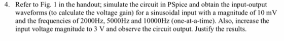
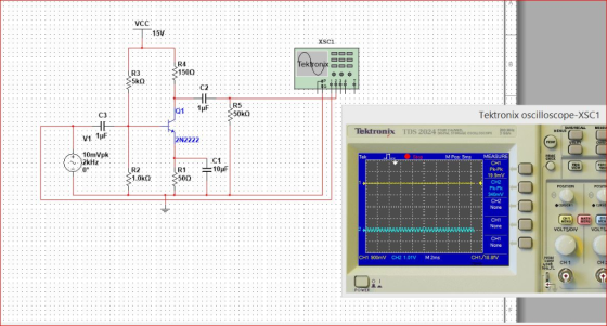
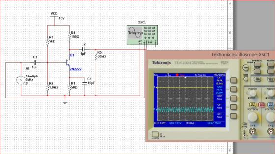
4. Refer to Fig. 1 in the handout; simulate the circuit in PSpice and obtain the input-output waveforms (to calculate the voltage gain) for a sinusoidal input with a magnitude of 10 mV and the frequencies of 2000Hz, 5000Hz and 10000Hz (one-at-a-time). Also, increase the input voltage magnitude to 3 V and observe the circuit output. Justify the results.
Homework Answers

 here
first 3 cases with input 10mV and next 3 cases with input 3V in the
second case you can observe the harmonic distortion in positive
side.
here
first 3 cases with input 10mV and next 3 cases with input 3V in the
second case you can observe the harmonic distortion in positive
side.
do not answer it , if you do not know how to use pspice Vc 15Vdc...
 do not answer it , if you do not know how to use pspice
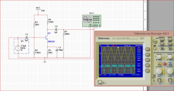
Vc 15Vdc R2 Rc 5k 150 C2 01 C1 RL 02N2222 Vin 50k R1 Re VAMP L-50mV FREQ 5000Hz Ce 10uF 1k 50 Figure 1: A Common-Emitter Amplifier Circuit Configuration 4. Refer to Fig. 1 in the handout; simulate the circuit in PSpice and obtain the input-output waveforms (to calculate the voltage gain) for a sinusoidal input with a magnitude of 10 mV and the frequencies...
do not answer it , if you do not know how to use pspice
Vc 15Vdc R2 Rc 5k 150 C2 01 C1 RL 02N2222 Vin 50k R1 Re VAMP L-50mV FREQ 5000Hz Ce 10uF 1k 50 Figure 1: A Common-Emitter Amplifier Circuit Configuration 4. Refer to Fig. 1 in the handout; simulate the circuit in PSpice and obtain the input-output waveforms (to calculate the voltage gain) for a sinusoidal input with a magnitude of 10 mV and the frequencies...
Refer to Fig. 5 in the handout; obtain the circuit output in PSpice for two input voltage sources...
 Refer to Fig. 5 in the handout; obtain the circuit output in PSpice for two input voltage sources (Va and Vb, different combinations of waveforms, amplitudes and frequencies) for the below resistor values 6. i. Ra-5K , Rb-5K, Rc=5K, Rd=10K. ii. Ra-10K, Rb-15K, Rc-5K, Rd-10K Also, analytically calculate the output voltage expression for the part-ii, only. Figure 5: A difference op-amp circuit.
Refer to Fig. 5 in the handout; obtain the circuit output in PSpice for two input voltage sources...
Refer to Fig. 5 in the handout; obtain the circuit output in PSpice for two input voltage sources (Va and Vb, different combinations of waveforms, amplitudes and frequencies) for the below resistor values 6. i. Ra-5K , Rb-5K, Rc=5K, Rd=10K. ii. Ra-10K, Rb-15K, Rc-5K, Rd-10K Also, analytically calculate the output voltage expression for the part-ii, only. Figure 5: A difference op-amp circuit.
Refer to Fig. 5 in the handout; obtain the circuit output in PSpice for two input voltage sources...
plz do not answer it , if you do not know how to use pspice 3. Refer to Fig. 1 in the handout; obtain the circuit output in PSpice for some of the digital input combinations given in Table. 1....
 plz do not answer it , if you do not know how to use
pspice
3. Refer to Fig. 1 in the handout; obtain the circuit output in PSpice for some of the digital input combinations given in Table. 1. Assume that 5V analog input and 0V analog input correspond to a digital ‘1' and a digital .0', respectively, and that the DAC outputs are converted so that positive voltages are obtained. Also, a. What is the range, precision and...
plz do not answer it , if you do not know how to use
pspice
3. Refer to Fig. 1 in the handout; obtain the circuit output in PSpice for some of the digital input combinations given in Table. 1. Assume that 5V analog input and 0V analog input correspond to a digital ‘1' and a digital .0', respectively, and that the DAC outputs are converted so that positive voltages are obtained. Also, a. What is the range, precision and...
Part I: Inverting Amplifier Procedure: 1. Build the circuit model for inverting amplifier in PSpice with...
 Part I: Inverting Amplifier Procedure: 1. Build the circuit model for inverting amplifier in PSpice with the following parameters: Ri = 5 k 2, R2 = 20 ks2, V+ = 10 V, V-=-10 V. 2. Hand calculates the theoretical closed loop gain Vout/Vin of the circuit model. 3. Generate a triangular waveform for Vin with the amplitude of 1 V and the period of 1 ms. 4. Run simulation. a. Set circuit model parameters. i.e., for voltage source: click VPWL...
done on pspice thank you Part IV: Diode Rectifiers Procedure: 1. Build the circuit model for...
 done on pspice thank you
Part IV: Diode Rectifiers Procedure: 1. Build the circuit model for full-wave diode rectifier in PSpice as shown in Fig. 4. The value of the load resistor is 10 k22. The input AC voltage source (VSIN in PSpice) is configured at 100 Hz and 20 V (peak-to- peak) in sinusoidal waveform. O 10K V.(t) V(A) A Figure 4. Circuit configuration for full-wave diode rectifier 2. Run the simulation and save the input and output voltage...
done on pspice thank you
Part IV: Diode Rectifiers Procedure: 1. Build the circuit model for full-wave diode rectifier in PSpice as shown in Fig. 4. The value of the load resistor is 10 k22. The input AC voltage source (VSIN in PSpice) is configured at 100 Hz and 20 V (peak-to- peak) in sinusoidal waveform. O 10K V.(t) V(A) A Figure 4. Circuit configuration for full-wave diode rectifier 2. Run the simulation and save the input and output voltage...
please do as soon as possible an use PSPICE I just need the pspice part please...
 please do as soon as possible an use PSPICE I just need
the pspice part
please use Pspice
use pspice to slove
Resistors 1.0kΩ, 1.2KΩ, 1.5ΚΩ, 1.8ΚΩ, 2.2kΩ, 2.7KΩ, 3.3kΩ, 3.9kΩ, 4.7kΩ, 5.6kΩ, 6.8ΚΩ, 8.2kΩ, 10kΩ, 12kΩ, 15kΩ, 18kΩ, 22kΩ, 27kg, 33kΩ, 30kΩ, 47ΚΩ, 56kΩ, 68kΩ, 82kΩ, 100kΩ. 120kΩ, 150kΩ, 180kΩ, 220kΩ, 270kΩ, 330kΩ, 39kΟΩ, 470kΩ, 560kΩ ** Put 60% 11:42 AM You Just now Part B. Non-Inverting Amplifier. Deliverables - PSpice schematic and graph 1. Draw the circuit for...
please do as soon as possible an use PSPICE I just need
the pspice part
please use Pspice
use pspice to slove
Resistors 1.0kΩ, 1.2KΩ, 1.5ΚΩ, 1.8ΚΩ, 2.2kΩ, 2.7KΩ, 3.3kΩ, 3.9kΩ, 4.7kΩ, 5.6kΩ, 6.8ΚΩ, 8.2kΩ, 10kΩ, 12kΩ, 15kΩ, 18kΩ, 22kΩ, 27kg, 33kΩ, 30kΩ, 47ΚΩ, 56kΩ, 68kΩ, 82kΩ, 100kΩ. 120kΩ, 150kΩ, 180kΩ, 220kΩ, 270kΩ, 330kΩ, 39kΟΩ, 470kΩ, 560kΩ ** Put 60% 11:42 AM You Just now Part B. Non-Inverting Amplifier. Deliverables - PSpice schematic and graph 1. Draw the circuit for...
please I need details l and....Debate Club | Offic A) Theoretical Design Design a common emitter BJT amplifier with the following requirements: -Rin-10 K2, and Ro-45 ㏀ (Neglect the Early voltage...
 please I need details
l and....Debate Club | Offic A) Theoretical Design Design a common emitter BJT amplifier with the following requirements: -Rin-10 K2, and Ro-45 ㏀ (Neglect the Early voltage Effect) Vo/Vsig- Gv-40 VIV or 32 dB " VCC-9 V V, IC-1mA, VCE-3.25V and β-100 RL-40 kQ, Rsige I ka, R 1-3R2, and C1-C2-1 μF Voc RC C2 R1 Rsig C1 RL R2 RE B) Verify your design using Orcad Capture Pspice by doing 1) AC sweep (frequency response):...
please I need details
l and....Debate Club | Offic A) Theoretical Design Design a common emitter BJT amplifier with the following requirements: -Rin-10 K2, and Ro-45 ㏀ (Neglect the Early voltage Effect) Vo/Vsig- Gv-40 VIV or 32 dB " VCC-9 V V, IC-1mA, VCE-3.25V and β-100 RL-40 kQ, Rsige I ka, R 1-3R2, and C1-C2-1 μF Voc RC C2 R1 Rsig C1 RL R2 RE B) Verify your design using Orcad Capture Pspice by doing 1) AC sweep (frequency response):...
how to draw this circuit in pspice PRE-LAB Resistors 150kQ, 180k2, 220k2, 270k2, 330k2, 39k02, 470k2, 560kQ Part A. I...
 how to draw this circuit in pspice
PRE-LAB Resistors 150kQ, 180k2, 220k2, 270k2, 330k2, 39k02, 470k2, 560kQ Part A. Inverting Amplifier. Deliverables - PSpice schematie and graphs 1. Draw the circuit for a standard inverting amplifier (see text). You can leave the resistors variables for now: Ai 2. Choose the resistor values from components available for this lab in the list above to give a gain between 5 and 10. Use values of 5.6 kΩ or greater. Record the resistor...
how to draw this circuit in pspice
PRE-LAB Resistors 150kQ, 180k2, 220k2, 270k2, 330k2, 39k02, 470k2, 560kQ Part A. Inverting Amplifier. Deliverables - PSpice schematie and graphs 1. Draw the circuit for a standard inverting amplifier (see text). You can leave the resistors variables for now: Ai 2. Choose the resistor values from components available for this lab in the list above to give a gain between 5 and 10. Use values of 5.6 kΩ or greater. Record the resistor...
Electronics-common emmitter amplifier. Pls be try to be helpful Im trying to study here in this book example.. However im kinda lost and i cant follow the correct answers they got.. could someon...
 Electronics-common emmitter amplifier. Pls be try to be
helpful
Im trying to study here in this book example..
However im kinda lost and i cant follow the correct answers
they got.. could someone pls help me..
I just wanna learn this, i hope u can help me learn by showin
clear and corect solutions on how to properly got the
answer..
Also especially on finding the values on the laod line
analysis, im lost.
Pls help
Any helpful help would...
Electronics-common emmitter amplifier. Pls be try to be
helpful
Im trying to study here in this book example..
However im kinda lost and i cant follow the correct answers
they got.. could someone pls help me..
I just wanna learn this, i hope u can help me learn by showin
clear and corect solutions on how to properly got the
answer..
Also especially on finding the values on the laod line
analysis, im lost.
Pls help
Any helpful help would...
You can use any software of your choice Begin by connecting the waveform generator to the...
 You can use any software of your choice
Begin by connecting the waveform generator to the series combination of a 0.2uF capacitor (use a decade capacitor box) and a 1 ks resistor (use a decade resistor box). Generate a 500 Hz, 8 Vp- p square wave with a 4 Volt offset and observe this waveform on the oscilloscope's Channel 1. Monitor the voltage drop across the capacitor on Channel 2. Figure 1 shows the schematic for the RC circuit 1k...
You can use any software of your choice
Begin by connecting the waveform generator to the series combination of a 0.2uF capacitor (use a decade capacitor box) and a 1 ks resistor (use a decade resistor box). Generate a 500 Hz, 8 Vp- p square wave with a 4 Volt offset and observe this waveform on the oscilloscope's Channel 1. Monitor the voltage drop across the capacitor on Channel 2. Figure 1 shows the schematic for the RC circuit 1k...
 do not answer it , if you do not know how to use pspice
Vc 15Vdc R2 Rc 5k 150 C2 01 C1 RL 02N2222 Vin 50k R1 Re VAMP L-50mV FREQ 5000Hz Ce 10uF 1k 50 Figure 1: A Common-Emitter Amplifier Circuit Configuration 4. Refer to Fig. 1 in the handout; simulate the circuit in PSpice and obtain the input-output waveforms (to calculate the voltage gain) for a sinusoidal input with a magnitude of 10 mV and the frequencies...
do not answer it , if you do not know how to use pspice
Vc 15Vdc R2 Rc 5k 150 C2 01 C1 RL 02N2222 Vin 50k R1 Re VAMP L-50mV FREQ 5000Hz Ce 10uF 1k 50 Figure 1: A Common-Emitter Amplifier Circuit Configuration 4. Refer to Fig. 1 in the handout; simulate the circuit in PSpice and obtain the input-output waveforms (to calculate the voltage gain) for a sinusoidal input with a magnitude of 10 mV and the frequencies...
 Refer to Fig. 5 in the handout; obtain the circuit output in PSpice for two input voltage sources (Va and Vb, different combinations of waveforms, amplitudes and frequencies) for the below resistor values 6. i. Ra-5K , Rb-5K, Rc=5K, Rd=10K. ii. Ra-10K, Rb-15K, Rc-5K, Rd-10K Also, analytically calculate the output voltage expression for the part-ii, only. Figure 5: A difference op-amp circuit.
Refer to Fig. 5 in the handout; obtain the circuit output in PSpice for two input voltage sources...
Refer to Fig. 5 in the handout; obtain the circuit output in PSpice for two input voltage sources (Va and Vb, different combinations of waveforms, amplitudes and frequencies) for the below resistor values 6. i. Ra-5K , Rb-5K, Rc=5K, Rd=10K. ii. Ra-10K, Rb-15K, Rc-5K, Rd-10K Also, analytically calculate the output voltage expression for the part-ii, only. Figure 5: A difference op-amp circuit.
Refer to Fig. 5 in the handout; obtain the circuit output in PSpice for two input voltage sources...
 plz do not answer it , if you do not know how to use
pspice
3. Refer to Fig. 1 in the handout; obtain the circuit output in PSpice for some of the digital input combinations given in Table. 1. Assume that 5V analog input and 0V analog input correspond to a digital ‘1' and a digital .0', respectively, and that the DAC outputs are converted so that positive voltages are obtained. Also, a. What is the range, precision and...
plz do not answer it , if you do not know how to use
pspice
3. Refer to Fig. 1 in the handout; obtain the circuit output in PSpice for some of the digital input combinations given in Table. 1. Assume that 5V analog input and 0V analog input correspond to a digital ‘1' and a digital .0', respectively, and that the DAC outputs are converted so that positive voltages are obtained. Also, a. What is the range, precision and...
 Part I: Inverting Amplifier Procedure: 1. Build the circuit model for inverting amplifier in PSpice with the following parameters: Ri = 5 k 2, R2 = 20 ks2, V+ = 10 V, V-=-10 V. 2. Hand calculates the theoretical closed loop gain Vout/Vin of the circuit model. 3. Generate a triangular waveform for Vin with the amplitude of 1 V and the period of 1 ms. 4. Run simulation. a. Set circuit model parameters. i.e., for voltage source: click VPWL...
 done on pspice thank you
Part IV: Diode Rectifiers Procedure: 1. Build the circuit model for full-wave diode rectifier in PSpice as shown in Fig. 4. The value of the load resistor is 10 k22. The input AC voltage source (VSIN in PSpice) is configured at 100 Hz and 20 V (peak-to- peak) in sinusoidal waveform. O 10K V.(t) V(A) A Figure 4. Circuit configuration for full-wave diode rectifier 2. Run the simulation and save the input and output voltage...
done on pspice thank you
Part IV: Diode Rectifiers Procedure: 1. Build the circuit model for full-wave diode rectifier in PSpice as shown in Fig. 4. The value of the load resistor is 10 k22. The input AC voltage source (VSIN in PSpice) is configured at 100 Hz and 20 V (peak-to- peak) in sinusoidal waveform. O 10K V.(t) V(A) A Figure 4. Circuit configuration for full-wave diode rectifier 2. Run the simulation and save the input and output voltage...
 please do as soon as possible an use PSPICE I just need
the pspice part
please use Pspice
use pspice to slove
Resistors 1.0kΩ, 1.2KΩ, 1.5ΚΩ, 1.8ΚΩ, 2.2kΩ, 2.7KΩ, 3.3kΩ, 3.9kΩ, 4.7kΩ, 5.6kΩ, 6.8ΚΩ, 8.2kΩ, 10kΩ, 12kΩ, 15kΩ, 18kΩ, 22kΩ, 27kg, 33kΩ, 30kΩ, 47ΚΩ, 56kΩ, 68kΩ, 82kΩ, 100kΩ. 120kΩ, 150kΩ, 180kΩ, 220kΩ, 270kΩ, 330kΩ, 39kΟΩ, 470kΩ, 560kΩ ** Put 60% 11:42 AM You Just now Part B. Non-Inverting Amplifier. Deliverables - PSpice schematic and graph 1. Draw the circuit for...
please do as soon as possible an use PSPICE I just need
the pspice part
please use Pspice
use pspice to slove
Resistors 1.0kΩ, 1.2KΩ, 1.5ΚΩ, 1.8ΚΩ, 2.2kΩ, 2.7KΩ, 3.3kΩ, 3.9kΩ, 4.7kΩ, 5.6kΩ, 6.8ΚΩ, 8.2kΩ, 10kΩ, 12kΩ, 15kΩ, 18kΩ, 22kΩ, 27kg, 33kΩ, 30kΩ, 47ΚΩ, 56kΩ, 68kΩ, 82kΩ, 100kΩ. 120kΩ, 150kΩ, 180kΩ, 220kΩ, 270kΩ, 330kΩ, 39kΟΩ, 470kΩ, 560kΩ ** Put 60% 11:42 AM You Just now Part B. Non-Inverting Amplifier. Deliverables - PSpice schematic and graph 1. Draw the circuit for...
 please I need details
l and....Debate Club | Offic A) Theoretical Design Design a common emitter BJT amplifier with the following requirements: -Rin-10 K2, and Ro-45 ㏀ (Neglect the Early voltage Effect) Vo/Vsig- Gv-40 VIV or 32 dB " VCC-9 V V, IC-1mA, VCE-3.25V and β-100 RL-40 kQ, Rsige I ka, R 1-3R2, and C1-C2-1 μF Voc RC C2 R1 Rsig C1 RL R2 RE B) Verify your design using Orcad Capture Pspice by doing 1) AC sweep (frequency response):...
please I need details
l and....Debate Club | Offic A) Theoretical Design Design a common emitter BJT amplifier with the following requirements: -Rin-10 K2, and Ro-45 ㏀ (Neglect the Early voltage Effect) Vo/Vsig- Gv-40 VIV or 32 dB " VCC-9 V V, IC-1mA, VCE-3.25V and β-100 RL-40 kQ, Rsige I ka, R 1-3R2, and C1-C2-1 μF Voc RC C2 R1 Rsig C1 RL R2 RE B) Verify your design using Orcad Capture Pspice by doing 1) AC sweep (frequency response):...
 how to draw this circuit in pspice
PRE-LAB Resistors 150kQ, 180k2, 220k2, 270k2, 330k2, 39k02, 470k2, 560kQ Part A. Inverting Amplifier. Deliverables - PSpice schematie and graphs 1. Draw the circuit for a standard inverting amplifier (see text). You can leave the resistors variables for now: Ai 2. Choose the resistor values from components available for this lab in the list above to give a gain between 5 and 10. Use values of 5.6 kΩ or greater. Record the resistor...
how to draw this circuit in pspice
PRE-LAB Resistors 150kQ, 180k2, 220k2, 270k2, 330k2, 39k02, 470k2, 560kQ Part A. Inverting Amplifier. Deliverables - PSpice schematie and graphs 1. Draw the circuit for a standard inverting amplifier (see text). You can leave the resistors variables for now: Ai 2. Choose the resistor values from components available for this lab in the list above to give a gain between 5 and 10. Use values of 5.6 kΩ or greater. Record the resistor...
 Electronics-common emmitter amplifier. Pls be try to be
helpful
Im trying to study here in this book example..
However im kinda lost and i cant follow the correct answers
they got.. could someone pls help me..
I just wanna learn this, i hope u can help me learn by showin
clear and corect solutions on how to properly got the
answer..
Also especially on finding the values on the laod line
analysis, im lost.
Pls help
Any helpful help would...
Electronics-common emmitter amplifier. Pls be try to be
helpful
Im trying to study here in this book example..
However im kinda lost and i cant follow the correct answers
they got.. could someone pls help me..
I just wanna learn this, i hope u can help me learn by showin
clear and corect solutions on how to properly got the
answer..
Also especially on finding the values on the laod line
analysis, im lost.
Pls help
Any helpful help would...
 You can use any software of your choice
Begin by connecting the waveform generator to the series combination of a 0.2uF capacitor (use a decade capacitor box) and a 1 ks resistor (use a decade resistor box). Generate a 500 Hz, 8 Vp- p square wave with a 4 Volt offset and observe this waveform on the oscilloscope's Channel 1. Monitor the voltage drop across the capacitor on Channel 2. Figure 1 shows the schematic for the RC circuit 1k...
You can use any software of your choice
Begin by connecting the waveform generator to the series combination of a 0.2uF capacitor (use a decade capacitor box) and a 1 ks resistor (use a decade resistor box). Generate a 500 Hz, 8 Vp- p square wave with a 4 Volt offset and observe this waveform on the oscilloscope's Channel 1. Monitor the voltage drop across the capacitor on Channel 2. Figure 1 shows the schematic for the RC circuit 1k...
Most questions answered within 3 hours.
-
Why is QE a controversial monetary policy tool.
A. It may lead to excessive inflation.B. By...
asked 14 minutes ago -
A finite potential well has depth U0 = 2.78 eV . What is the
penetration distance...
asked 39 minutes ago -
1. The bus bars of a power station are in two sections A and B
separated...
asked 38 minutes ago -
Fiscal policy is the deliberate manipulation of taxes and
government spending to alter GDP, employment, inflation...
asked 1 hour ago -
evaluating an expression using only one digit and + and - as
operators ....3+5-1+7-5+8
-----------------------
stack...
asked 1 hour ago -
Two concentric current loops lie in the same plane. The smaller
loop has a radius of...
asked 2 hours ago -
1)Which of the following is an
important difference between qualified and nonqualified retirement
plans?
a. Qualified...
asked 2 hours ago -
What's the streaming business's problem on the
horizon?
asked 3 hours ago -
I need help with writing the conclusion for this online lab
report
Abstract
By testing the...
asked 3 hours ago -
For the reaction 1N2+3H2-----> 2NH3, would the reaction rate
trend be: delta[NH3]/ delta t = -2...
asked 3 hours ago -
Within your current/past organization, identify a problem/issue
and format a design to address same. You may...
asked 3 hours ago -
A sock stuck to the side of a clothes-dryer barrel has a
centripetal acceleration of 24...
asked 4 hours ago