
Homework Answers
Add Answer to:
how to draw this circuit in pspice PRE-LAB Resistors 150kQ, 180k2, 220k2, 270k2, 330k2, 39k02, 470k2, 560kQ Part A. I...
please do as soon as possible an use PSPICE I just need the pspice part please...
 please do as soon as possible an use PSPICE I just need
the pspice part
please use Pspice
use pspice to slove
Resistors 1.0kΩ, 1.2KΩ, 1.5ΚΩ, 1.8ΚΩ, 2.2kΩ, 2.7KΩ, 3.3kΩ, 3.9kΩ, 4.7kΩ, 5.6kΩ, 6.8ΚΩ, 8.2kΩ, 10kΩ, 12kΩ, 15kΩ, 18kΩ, 22kΩ, 27kg, 33kΩ, 30kΩ, 47ΚΩ, 56kΩ, 68kΩ, 82kΩ, 100kΩ. 120kΩ, 150kΩ, 180kΩ, 220kΩ, 270kΩ, 330kΩ, 39kΟΩ, 470kΩ, 560kΩ ** Put 60% 11:42 AM You Just now Part B. Non-Inverting Amplifier. Deliverables - PSpice schematic and graph 1. Draw the circuit for...
please do as soon as possible an use PSPICE I just need
the pspice part
please use Pspice
use pspice to slove
Resistors 1.0kΩ, 1.2KΩ, 1.5ΚΩ, 1.8ΚΩ, 2.2kΩ, 2.7KΩ, 3.3kΩ, 3.9kΩ, 4.7kΩ, 5.6kΩ, 6.8ΚΩ, 8.2kΩ, 10kΩ, 12kΩ, 15kΩ, 18kΩ, 22kΩ, 27kg, 33kΩ, 30kΩ, 47ΚΩ, 56kΩ, 68kΩ, 82kΩ, 100kΩ. 120kΩ, 150kΩ, 180kΩ, 220kΩ, 270kΩ, 330kΩ, 39kΟΩ, 470kΩ, 560kΩ ** Put 60% 11:42 AM You Just now Part B. Non-Inverting Amplifier. Deliverables - PSpice schematic and graph 1. Draw the circuit for...
2. Design a non-inverting op-amp circuit with two resistors under the following conditions: a. The gain of the ampl...
 2. Design a non-inverting op-amp circuit with two resistors under the following conditions: a. The gain of the amplifier must be +10 b. The input range is ± 2V c. The total power consumed by the resistors must be less than 100 mW Show all the calculations required to design the amplifier circuit with the shown specifications.in details Use MULTISIM to create the op-amp circuit and print a fully labelled diagram of the circuits with the voltmeters displays showing both...
Part I: Inverting Amplifier Procedure: 1. Build the circuit model for inverting amplifier in PSpice with...
 Part I: Inverting Amplifier Procedure: 1. Build the circuit model for inverting amplifier in PSpice with the following parameters: Ri = 5 k 2, R2 = 20 ks2, V+ = 10 V, V-=-10 V. 2. Hand calculates the theoretical closed loop gain Vout/Vin of the circuit model. 3. Generate a triangular waveform for Vin with the amplitude of 1 V and the period of 1 ms. 4. Run simulation. a. Set circuit model parameters. i.e., for voltage source: click VPWL...
3- OPERATIONAL-AMPLIFIER Nominating ampliar Voltage Show OW Difference ampliar Wate Date amplizier Close R Vout Voutin...
 3- OPERATIONAL-AMPLIFIER Nominating ampliar Voltage Show OW Difference ampliar Wate Date amplizier Close R Vout Voutin Vout = vin Buffer = Inverting amplifier Dout = (1 + .. Vout V out 1 V2 ERR Vour (, - v3) Differential Amplifier Non-Inverting amplifier 1- Refer to the op amp in Fig. If v; = 0.5 V, calculate: (a) the output voltage Vos (b) the current in the 10-k! resistor. 25k92 10k02 Oo + 6 2. A 741 op amp has an...
The gain of the non-inverting amplifier is set by the values of the resistors connected to the op...
 The gain of the non-inverting amplifier is set by the values of the resistors connected to the op- .amp can never be less than 1, even when RB is very high and RT equals 0 A voltage divider is a circuit involving two resistors in series All above is .1 correct Which statement not correct for Ideal operational amplifier Infinite open loop gain AOL for differential .1 .signa Zero gain for the common mode signal .Zero output impedance .noninfinite bandwidth...
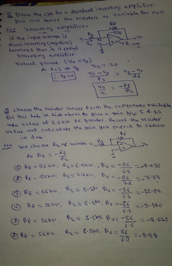
A. (10 pts) Implement the voltage amplifier shown below using an ideal op amp circuit. You have o...
 a. (10 pts) Implement the voltage amplifier shown below using an ideal op amp circuit. You have one op amp available for this circuit, and a range of resistors with values from 1 kΩ to 100 ka. Draw the schematic of your op amp circuit, labeling resistor values. Make sure the gain, input resistance, and output resistance of your circuit matches the model in the schematic. R=012 *100v, RL 100 b. (5 pts) Your amplifier circuit should have a frequency...
I need help to find the values! gures below (a-d), determine the values for R1, R2, voltage or type of op-amp based on the information listed. You may ors with an open circuit, short circuit, or v...
 I need help to find the values!
gures below (a-d), determine the values for R1, R2, voltage or type of op-amp based on the information listed. You may ors with an open circuit, short circuit, or values 1kn SRS1Mn. gain, voltage, a) 76 k2 Type: Non-Inverting Vout max R1 (based on Voutmas) 0.3V Type: Inverting, Av =-100 V/V Vin- b) R1 12V R1 12V Type: Buffer Vout- R1 =- c) +10 V R1 ーVout -10 V Type: Av- IV R2...
I need help to find the values!
gures below (a-d), determine the values for R1, R2, voltage or type of op-amp based on the information listed. You may ors with an open circuit, short circuit, or values 1kn SRS1Mn. gain, voltage, a) 76 k2 Type: Non-Inverting Vout max R1 (based on Voutmas) 0.3V Type: Inverting, Av =-100 V/V Vin- b) R1 12V R1 12V Type: Buffer Vout- R1 =- c) +10 V R1 ーVout -10 V Type: Av- IV R2...
Inverting Amplifier Figure 4.2 shows the fundamental configuration of Op-Amp in which it is used as...
 Inverting Amplifier Figure 4.2 shows the fundamental configuration of Op-Amp in which it is used as an inverting amplifier. In this configuration the ratio, R2/R1 completely controls the effective gain of the amplifier and it can be verified that the output voltage is equal to Vo = - (R2/R1)Vin R2 100K Q-10V R1 Vinow 20K 1 2 7 V Vo 3 -10v Figure 4.2 Part 1 - Inverting Amp: Procedure 1. Construct the circuit of figure 4.2 using Op-Amp IC...
Find the induction process of A, β, Ro, Ri. EXAMPLE 10.10 Figure 10.27 shows a feedback current amplifier formed by cas...
 Find the induction process of A, β, Ro, Ri.
EXAMPLE 10.10 Figure 10.27 shows a feedback current amplifier formed by cascading an inverting voltage amplifier u witha MOSFET Q. The output current I, is the drain current of Q. The feedback network, consisting of resistors R, and R, senses an exactly equal current, namely, the source current of Q, and provides feedback current signal that is mixed with I, at the input node. Note that the bias arrangement is not...
Find the induction process of A, β, Ro, Ri.
EXAMPLE 10.10 Figure 10.27 shows a feedback current amplifier formed by cascading an inverting voltage amplifier u witha MOSFET Q. The output current I, is the drain current of Q. The feedback network, consisting of resistors R, and R, senses an exactly equal current, namely, the source current of Q, and provides feedback current signal that is mixed with I, at the input node. Note that the bias arrangement is not...
Assuming an ideal op-amp, design an inverting amplifier with a gain of 26 dB
Assuming an ideal op-amp, design an inverting amplifier with a gain of 26 dB having the largest possible R1 value under the constraint of having to use resistors no larger than 1 MΩ. If the input voltage source of this amplifier has an internal resistance r0 = 50 kΩ, how will this affect the gain? Design a solution that will eliminate the effect of the internal source resistance without having to change the values of R1 and R2.
 please do as soon as possible an use PSPICE I just need
the pspice part
please use Pspice
use pspice to slove
Resistors 1.0kΩ, 1.2KΩ, 1.5ΚΩ, 1.8ΚΩ, 2.2kΩ, 2.7KΩ, 3.3kΩ, 3.9kΩ, 4.7kΩ, 5.6kΩ, 6.8ΚΩ, 8.2kΩ, 10kΩ, 12kΩ, 15kΩ, 18kΩ, 22kΩ, 27kg, 33kΩ, 30kΩ, 47ΚΩ, 56kΩ, 68kΩ, 82kΩ, 100kΩ. 120kΩ, 150kΩ, 180kΩ, 220kΩ, 270kΩ, 330kΩ, 39kΟΩ, 470kΩ, 560kΩ ** Put 60% 11:42 AM You Just now Part B. Non-Inverting Amplifier. Deliverables - PSpice schematic and graph 1. Draw the circuit for...
please do as soon as possible an use PSPICE I just need
the pspice part
please use Pspice
use pspice to slove
Resistors 1.0kΩ, 1.2KΩ, 1.5ΚΩ, 1.8ΚΩ, 2.2kΩ, 2.7KΩ, 3.3kΩ, 3.9kΩ, 4.7kΩ, 5.6kΩ, 6.8ΚΩ, 8.2kΩ, 10kΩ, 12kΩ, 15kΩ, 18kΩ, 22kΩ, 27kg, 33kΩ, 30kΩ, 47ΚΩ, 56kΩ, 68kΩ, 82kΩ, 100kΩ. 120kΩ, 150kΩ, 180kΩ, 220kΩ, 270kΩ, 330kΩ, 39kΟΩ, 470kΩ, 560kΩ ** Put 60% 11:42 AM You Just now Part B. Non-Inverting Amplifier. Deliverables - PSpice schematic and graph 1. Draw the circuit for...
 2. Design a non-inverting op-amp circuit with two resistors under the following conditions: a. The gain of the amplifier must be +10 b. The input range is ± 2V c. The total power consumed by the resistors must be less than 100 mW Show all the calculations required to design the amplifier circuit with the shown specifications.in details Use MULTISIM to create the op-amp circuit and print a fully labelled diagram of the circuits with the voltmeters displays showing both...
 Part I: Inverting Amplifier Procedure: 1. Build the circuit model for inverting amplifier in PSpice with the following parameters: Ri = 5 k 2, R2 = 20 ks2, V+ = 10 V, V-=-10 V. 2. Hand calculates the theoretical closed loop gain Vout/Vin of the circuit model. 3. Generate a triangular waveform for Vin with the amplitude of 1 V and the period of 1 ms. 4. Run simulation. a. Set circuit model parameters. i.e., for voltage source: click VPWL...
 3- OPERATIONAL-AMPLIFIER Nominating ampliar Voltage Show OW Difference ampliar Wate Date amplizier Close R Vout Voutin Vout = vin Buffer = Inverting amplifier Dout = (1 + .. Vout V out 1 V2 ERR Vour (, - v3) Differential Amplifier Non-Inverting amplifier 1- Refer to the op amp in Fig. If v; = 0.5 V, calculate: (a) the output voltage Vos (b) the current in the 10-k! resistor. 25k92 10k02 Oo + 6 2. A 741 op amp has an...
 The gain of the non-inverting amplifier is set by the values of the resistors connected to the op- .amp can never be less than 1, even when RB is very high and RT equals 0 A voltage divider is a circuit involving two resistors in series All above is .1 correct Which statement not correct for Ideal operational amplifier Infinite open loop gain AOL for differential .1 .signa Zero gain for the common mode signal .Zero output impedance .noninfinite bandwidth...
 a. (10 pts) Implement the voltage amplifier shown below using an ideal op amp circuit. You have one op amp available for this circuit, and a range of resistors with values from 1 kΩ to 100 ka. Draw the schematic of your op amp circuit, labeling resistor values. Make sure the gain, input resistance, and output resistance of your circuit matches the model in the schematic. R=012 *100v, RL 100 b. (5 pts) Your amplifier circuit should have a frequency...
 I need help to find the values!
gures below (a-d), determine the values for R1, R2, voltage or type of op-amp based on the information listed. You may ors with an open circuit, short circuit, or values 1kn SRS1Mn. gain, voltage, a) 76 k2 Type: Non-Inverting Vout max R1 (based on Voutmas) 0.3V Type: Inverting, Av =-100 V/V Vin- b) R1 12V R1 12V Type: Buffer Vout- R1 =- c) +10 V R1 ーVout -10 V Type: Av- IV R2...
I need help to find the values!
gures below (a-d), determine the values for R1, R2, voltage or type of op-amp based on the information listed. You may ors with an open circuit, short circuit, or values 1kn SRS1Mn. gain, voltage, a) 76 k2 Type: Non-Inverting Vout max R1 (based on Voutmas) 0.3V Type: Inverting, Av =-100 V/V Vin- b) R1 12V R1 12V Type: Buffer Vout- R1 =- c) +10 V R1 ーVout -10 V Type: Av- IV R2...
 Inverting Amplifier Figure 4.2 shows the fundamental configuration of Op-Amp in which it is used as an inverting amplifier. In this configuration the ratio, R2/R1 completely controls the effective gain of the amplifier and it can be verified that the output voltage is equal to Vo = - (R2/R1)Vin R2 100K Q-10V R1 Vinow 20K 1 2 7 V Vo 3 -10v Figure 4.2 Part 1 - Inverting Amp: Procedure 1. Construct the circuit of figure 4.2 using Op-Amp IC...
 Find the induction process of A, β, Ro, Ri.
EXAMPLE 10.10 Figure 10.27 shows a feedback current amplifier formed by cascading an inverting voltage amplifier u witha MOSFET Q. The output current I, is the drain current of Q. The feedback network, consisting of resistors R, and R, senses an exactly equal current, namely, the source current of Q, and provides feedback current signal that is mixed with I, at the input node. Note that the bias arrangement is not...
Find the induction process of A, β, Ro, Ri.
EXAMPLE 10.10 Figure 10.27 shows a feedback current amplifier formed by cascading an inverting voltage amplifier u witha MOSFET Q. The output current I, is the drain current of Q. The feedback network, consisting of resistors R, and R, senses an exactly equal current, namely, the source current of Q, and provides feedback current signal that is mixed with I, at the input node. Note that the bias arrangement is not...
Most questions answered within 3 hours.
-
A university administrator working in student housing wants to
determine if the percentage of students residing...
asked 7 minutes ago -
3). Describe human population growth that has occurred in the
past 400 years. Use terms learned...
asked 4 minutes ago -
A
projectile is blue at a target. The distance from the point of
impact to the...
asked 29 minutes ago -
Given a 32 bit processor, with 2 MB of physical RAM split into 512
frames. What...
asked 19 minutes ago -
What were the main rulings in the Supreme Court cases which are
Morgan v. Virginia (1946)...
asked 18 minutes ago -
write a five paragraph essay on how setting,
specifically culture, influences the actions of
the characters...
asked 10 minutes ago -
JAVA
Provide a simple code sample of Merge sort
asked 21 minutes ago -
Discounting cash flows involves:
A. taking the cash discount offered on a trade merchandise
B. estimating...
asked 28 minutes ago -
A solid wood door 1.00 m wide and 2.00 m high is hinged along
one side...
asked 28 minutes ago -
Raleigh Company manufactures two joint products. At the
split-off point, they have sales values of:
Product...
asked 28 minutes ago -
1. Your grandmother has invested $4000 in a mutual fund each
year on your birthday (she...
asked 30 minutes ago -
HELP WITH SAS
Run the following DATA step to create a SAS data set called
ABC_CORP....
asked 43 minutes ago