Please explain all steps and reasoning!
Homework Answers


Add Answer to:
Please explain all steps and reasoning!
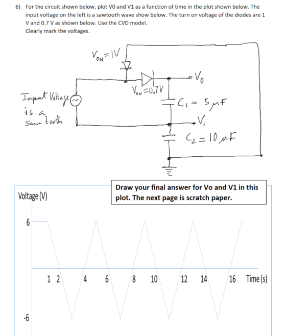
6) For the circuit shown below, plot VO and V1...
Please explain all steps and reasoning! 6) For the circuit shown below, plot VO and V1...
 Please explain all steps and reasoning!
6) For the circuit shown below, plot VO and V1 as a function of time in the plot shown below. The input voltage on the left is a sawtooth wave show below. The turn on voltage of the diodes are 1 V and 0.7 V as shown below. Use the CVD model Clearly mark the voltages. VNIV OD 0.7V Tapat Villay V San 210 mF Draw your final answer for Vo and V1 in...
Please explain all steps and reasoning!
6) For the circuit shown below, plot VO and V1 as a function of time in the plot shown below. The input voltage on the left is a sawtooth wave show below. The turn on voltage of the diodes are 1 V and 0.7 V as shown below. Use the CVD model Clearly mark the voltages. VNIV OD 0.7V Tapat Villay V San 210 mF Draw your final answer for Vo and V1 in...
once simulated can tou explain what the diodes are doing ... please explain good thank you...
 once simulated can tou explain what the diodes are doing ...
please explain good thank you
Problem 1: Voltage Limiting 1.1. Simulate the following simple resistor-diode circuit (shown on the left in Figure 1) R1 V out V1 ZD1 VOFF 0 VAMPL 3V FREQ 1KHZ 0.7 D1N4148 Figure Let V(in) be a 1KHZ VSIN with an amplitude of 3V. RI is 1KO. Lowest node voltage is ground. (1.1a) Set up PSPICE Transient and plot both V(in) and V(out) on the...
once simulated can tou explain what the diodes are doing ...
please explain good thank you
Problem 1: Voltage Limiting 1.1. Simulate the following simple resistor-diode circuit (shown on the left in Figure 1) R1 V out V1 ZD1 VOFF 0 VAMPL 3V FREQ 1KHZ 0.7 D1N4148 Figure Let V(in) be a 1KHZ VSIN with an amplitude of 3V. RI is 1KO. Lowest node voltage is ground. (1.1a) Set up PSPICE Transient and plot both V(in) and V(out) on the...
For the fullwave rectifier circuit shown below, the input voltage is Vi 6 sin 2n60t and...
 For the fullwave rectifier circuit shown below, the input voltage is Vi 6 sin 2n60t and the diodes D1, D2, D3, D4 each have a forward- voltage drop of 0.7 V when conducting. Determine the average value of the output voltage Vo (in V). (Enter your answer as a number without the units.)
Figure 3. Variable RC circuit A variable time constant circuit is shown above. The potentiometer (R2)...
 Figure 3. Variable RC circuit A variable time constant circuit is shown above. The potentiometer (R2) can change its resistance from 0 Ohms to 750 Ohms. R1 has a fixed value of 70 Ohms. The capacitor has a capacitance of 35 pF. a) Use the supplied MATLAB™ code Calc RC and function RC_Circ to find the time variation of voltage across the Capacitor, Ve, and the fixed resistor R1 for a steady voltage V1 = 5 Volts which is turned...
Aufilo polasi For the op amp shown below, the output saturation voltages of the op amp...
 Aufilo polasi For the op amp shown below, the output saturation voltages of the op amp shown below is t 10 volts. In addition, assume that conducting 6. ( 16 points) the a conducting diode has a voltage drop of 0.7 volts. Furthermore, R- R-10 KQ (a) Ir v1.SV, find and v (b) If v, =-2.5 V, find Vo and va
For the double diode circuit shown in figure 2-1, answer the following questions. In Figure 2-1...
 For the double diode circuit shown in figure 2-1, answer the following questions. In Figure 2-1 a) (10pts) For the triangular wave input shown (Vin), sketch the output voltage (Vout) using the constant voltage drop model (CVD: Vo-0.7V). Be sure to note the voltage values on the y-axis of your Vout plot and show any equations you used to determine those values ime FEE 334: Spring 2019 Midterm b) (2pts) During the middle of the first time segment (when Vin...
Please show all of the steps Question 2: 20% We can use stack of diodes as...
 Please show all of the steps
Question 2: 20% We can use stack of diodes as a voltage regulator as shown in the circuit below. Consider input voltage to this circuit as 20V DC with IV of fluctuation. Diodes in this circuit have 0.7V forward voltage drop a) What is DC output voltage Vo? 20+1V Vo= 1.4 V R=1k2 b) What is diode DC current lo? Ip= 18-6 ma c) What is the value of individual diode's small-signal resistor/? (4%)...
Please show all of the steps
Question 2: 20% We can use stack of diodes as a voltage regulator as shown in the circuit below. Consider input voltage to this circuit as 20V DC with IV of fluctuation. Diodes in this circuit have 0.7V forward voltage drop a) What is DC output voltage Vo? 20+1V Vo= 1.4 V R=1k2 b) What is diode DC current lo? Ip= 18-6 ma c) What is the value of individual diode's small-signal resistor/? (4%)...
Consider the full-wave rectifier circuit below. Use a constant voltage drop model for the diodes with...
 Consider the full-wave rectifier circuit below. Use a constant voltage drop model for the diodes with VD 1. 0.7 V. Let v": 10 sin(2n(2000 and RI-100Q. (6 pt) Calelae the average vales of oun uinege D1 D4 V1 R1 with respect to time or angle. out b. (2+3 pts) A capacitor is placed across RI to reduce the ripple to D3 D2 20 mVp-p. Find the capacitor value. (2+3 pts) Calculate the approximate average Vout value assuming a 20 m...
Design a two-stage Op-Amp circuit as shown below to make the output voltage is vo=C1v1+C2v2, where...
 Design a two-stage Op-Amp circuit as shown below to make the
output voltage is
vo=C1v1+C2v2,
where C1 = 6 and C2 = 11.5, given that
Rf1=84 k?, and Rf2=21.5 k?.
a. Find the values of R1 and R2.
R1: _______ (k?); R2: _______ (k?)
b. Find the value of RS2:
_______(k?)
c. If v1=2.4 V and v2=3 V, find the output
voltage vo:
_______(V)
Rf Rf R2 02 Pi P2 Stage 1 Stage 2
Design a two-stage Op-Amp circuit as shown below to make the
output voltage is
vo=C1v1+C2v2,
where C1 = 6 and C2 = 11.5, given that
Rf1=84 k?, and Rf2=21.5 k?.
a. Find the values of R1 and R2.
R1: _______ (k?); R2: _______ (k?)
b. Find the value of RS2:
_______(k?)
c. If v1=2.4 V and v2=3 V, find the output
voltage vo:
_______(V)
Rf Rf R2 02 Pi P2 Stage 1 Stage 2
For the circuit shown below: In terms of Vo, R1, R2, R3, R4, C1, t, and s what is the time domain...
 For the circuit shown below: In terms of Vo, R1, R2, R3, R4, C1, t, and s what is the time domain equation for the voltage at node out? Preview In terms of Vo, R1, R2, ,R3, R4, C1, t, and s what is the s-domain equation for voltage at node out? In terms of Vo, RI, R2, R3, R4, CI, t, and s what is the equation for τ? If the voltage V1 at time-0 is 1 V R1-1...
 Please explain all steps and reasoning!
6) For the circuit shown below, plot VO and V1 as a function of time in the plot shown below. The input voltage on the left is a sawtooth wave show below. The turn on voltage of the diodes are 1 V and 0.7 V as shown below. Use the CVD model Clearly mark the voltages. VNIV OD 0.7V Tapat Villay V San 210 mF Draw your final answer for Vo and V1 in...
Please explain all steps and reasoning!
6) For the circuit shown below, plot VO and V1 as a function of time in the plot shown below. The input voltage on the left is a sawtooth wave show below. The turn on voltage of the diodes are 1 V and 0.7 V as shown below. Use the CVD model Clearly mark the voltages. VNIV OD 0.7V Tapat Villay V San 210 mF Draw your final answer for Vo and V1 in...
 once simulated can tou explain what the diodes are doing ...
please explain good thank you
Problem 1: Voltage Limiting 1.1. Simulate the following simple resistor-diode circuit (shown on the left in Figure 1) R1 V out V1 ZD1 VOFF 0 VAMPL 3V FREQ 1KHZ 0.7 D1N4148 Figure Let V(in) be a 1KHZ VSIN with an amplitude of 3V. RI is 1KO. Lowest node voltage is ground. (1.1a) Set up PSPICE Transient and plot both V(in) and V(out) on the...
once simulated can tou explain what the diodes are doing ...
please explain good thank you
Problem 1: Voltage Limiting 1.1. Simulate the following simple resistor-diode circuit (shown on the left in Figure 1) R1 V out V1 ZD1 VOFF 0 VAMPL 3V FREQ 1KHZ 0.7 D1N4148 Figure Let V(in) be a 1KHZ VSIN with an amplitude of 3V. RI is 1KO. Lowest node voltage is ground. (1.1a) Set up PSPICE Transient and plot both V(in) and V(out) on the...
 For the fullwave rectifier circuit shown below, the input voltage is Vi 6 sin 2n60t and the diodes D1, D2, D3, D4 each have a forward- voltage drop of 0.7 V when conducting. Determine the average value of the output voltage Vo (in V). (Enter your answer as a number without the units.)
 Figure 3. Variable RC circuit A variable time constant circuit is shown above. The potentiometer (R2) can change its resistance from 0 Ohms to 750 Ohms. R1 has a fixed value of 70 Ohms. The capacitor has a capacitance of 35 pF. a) Use the supplied MATLAB™ code Calc RC and function RC_Circ to find the time variation of voltage across the Capacitor, Ve, and the fixed resistor R1 for a steady voltage V1 = 5 Volts which is turned...
 Aufilo polasi For the op amp shown below, the output saturation voltages of the op amp shown below is t 10 volts. In addition, assume that conducting 6. ( 16 points) the a conducting diode has a voltage drop of 0.7 volts. Furthermore, R- R-10 KQ (a) Ir v1.SV, find and v (b) If v, =-2.5 V, find Vo and va
 For the double diode circuit shown in figure 2-1, answer the following questions. In Figure 2-1 a) (10pts) For the triangular wave input shown (Vin), sketch the output voltage (Vout) using the constant voltage drop model (CVD: Vo-0.7V). Be sure to note the voltage values on the y-axis of your Vout plot and show any equations you used to determine those values ime FEE 334: Spring 2019 Midterm b) (2pts) During the middle of the first time segment (when Vin...
 Please show all of the steps
Question 2: 20% We can use stack of diodes as a voltage regulator as shown in the circuit below. Consider input voltage to this circuit as 20V DC with IV of fluctuation. Diodes in this circuit have 0.7V forward voltage drop a) What is DC output voltage Vo? 20+1V Vo= 1.4 V R=1k2 b) What is diode DC current lo? Ip= 18-6 ma c) What is the value of individual diode's small-signal resistor/? (4%)...
Please show all of the steps
Question 2: 20% We can use stack of diodes as a voltage regulator as shown in the circuit below. Consider input voltage to this circuit as 20V DC with IV of fluctuation. Diodes in this circuit have 0.7V forward voltage drop a) What is DC output voltage Vo? 20+1V Vo= 1.4 V R=1k2 b) What is diode DC current lo? Ip= 18-6 ma c) What is the value of individual diode's small-signal resistor/? (4%)...
 Consider the full-wave rectifier circuit below. Use a constant voltage drop model for the diodes with VD 1. 0.7 V. Let v": 10 sin(2n(2000 and RI-100Q. (6 pt) Calelae the average vales of oun uinege D1 D4 V1 R1 with respect to time or angle. out b. (2+3 pts) A capacitor is placed across RI to reduce the ripple to D3 D2 20 mVp-p. Find the capacitor value. (2+3 pts) Calculate the approximate average Vout value assuming a 20 m...
 Design a two-stage Op-Amp circuit as shown below to make the
output voltage is
vo=C1v1+C2v2,
where C1 = 6 and C2 = 11.5, given that
Rf1=84 k?, and Rf2=21.5 k?.
a. Find the values of R1 and R2.
R1: _______ (k?); R2: _______ (k?)
b. Find the value of RS2:
_______(k?)
c. If v1=2.4 V and v2=3 V, find the output
voltage vo:
_______(V)
Rf Rf R2 02 Pi P2 Stage 1 Stage 2
Design a two-stage Op-Amp circuit as shown below to make the
output voltage is
vo=C1v1+C2v2,
where C1 = 6 and C2 = 11.5, given that
Rf1=84 k?, and Rf2=21.5 k?.
a. Find the values of R1 and R2.
R1: _______ (k?); R2: _______ (k?)
b. Find the value of RS2:
_______(k?)
c. If v1=2.4 V and v2=3 V, find the output
voltage vo:
_______(V)
Rf Rf R2 02 Pi P2 Stage 1 Stage 2
 For the circuit shown below: In terms of Vo, R1, R2, R3, R4, C1, t, and s what is the time domain equation for the voltage at node out? Preview In terms of Vo, R1, R2, ,R3, R4, C1, t, and s what is the s-domain equation for voltage at node out? In terms of Vo, RI, R2, R3, R4, CI, t, and s what is the equation for τ? If the voltage V1 at time-0 is 1 V R1-1...
Most questions answered within 3 hours.
-
Calculate the number density of argon gas at a temperature of
24C and a pressure of...
asked 43 minutes ago -
Alternative
Classification
How to Estimate
Probabilities from Data? ( For continuous Attributes)
And How to generate...
asked 46 minutes ago -
An explosion breaks a 20.0-kg object into three parts. The
object is initially moving at a...
asked 1 hour ago -
Calculate the approximate number of residues of Rubisco, which
is involved in carbon fixation in plants,...
asked 2 hours ago -
Other decisions about scientific claims can have a much broader
impact.ENERGYarrow-10x10.png, environment, health, security - all...
asked 3 hours ago -
I need to write a research paper and work cited about this
topic: The United States...
asked 3 hours ago -
Hello! I was wondering if I could have some help?
If the vapor pressure of carvone...
asked 4 hours ago -
An economist wants to estimate the mean per capita income (in
thousands of dollars) for a...
asked 4 hours ago -
What would be the input/output characteristic of a circuit
obtained by putting two of your 2's-complementers...
asked 4 hours ago -
In Drosophila, the transition from the syncytial blastoderm
stage to the cellular blastoderm stage is a...
asked 5 hours ago -
Project management question:
Name 3 different types of resources (hint: humans are one
type)
asked 5 hours ago -
Consider the following reaction: C 2H 2( g) + 2H 2( g) C 2H 6(
g)...
asked 5 hours ago