

Homework Answers
Add Answer to:
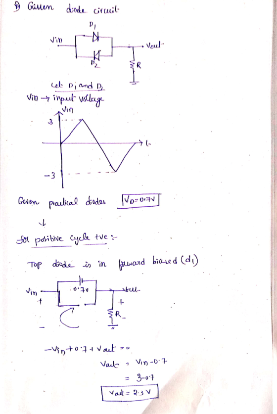
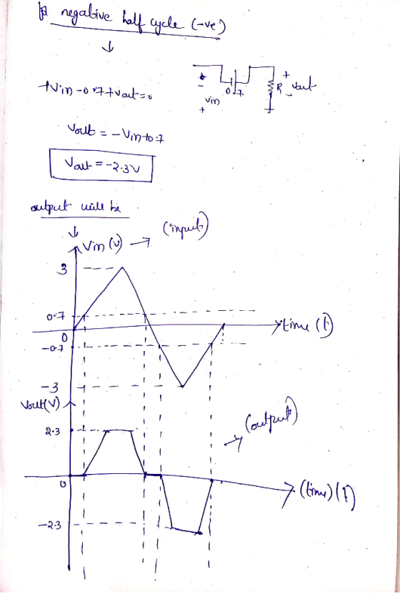
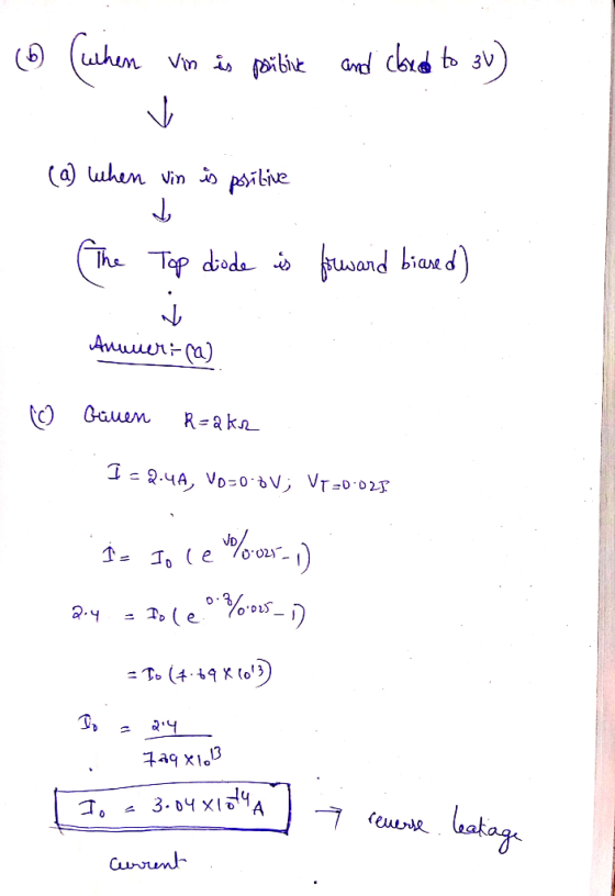
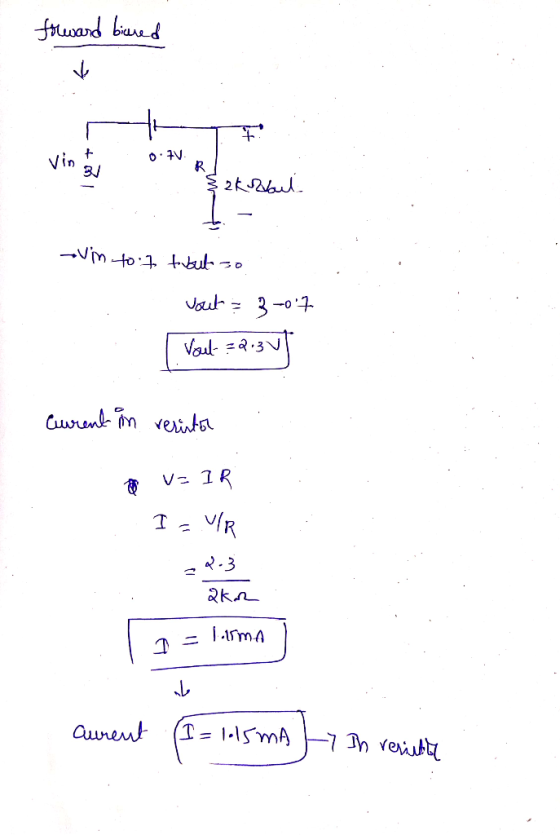
For the double diode circuit shown in figure 2-1, answer the following questions. In Figure 2-1...
For the diodes, use the models shown below; the regular diode model has 0.7V forward bias...
 For the diodes, use the models shown below; the regular diode
model has 0.7V forward bias voltage; the Zener diode model has -3V
breakdown voltage
Question 2 (25 points) For the diodes, use the models shown below; the regular diode model has 0.7V forward bias voltage; the Zener diode model has -3V breakdown voltage. a) Determine the minimum positive value of in to make D1 conduct current. (10 pts) b) Determine the minimum positive value of lin to make D2...
For the diodes, use the models shown below; the regular diode
model has 0.7V forward bias voltage; the Zener diode model has -3V
breakdown voltage
Question 2 (25 points) For the diodes, use the models shown below; the regular diode model has 0.7V forward bias voltage; the Zener diode model has -3V breakdown voltage. a) Determine the minimum positive value of in to make D1 conduct current. (10 pts) b) Determine the minimum positive value of lin to make D2...
a) Using the constant voltage drop (CVD) model, what is the minimum input voltage that can...
 a) Using the constant voltage
drop (CVD) model, what is the minimum input
voltage that can reach the MOS circuitry before a diode
turns on, shunting the current to ground? (At this point you
can assume R1 = R2 = 0Ω)
b) Using the constant voltage drop (CVD) model, what is the
maximum input voltage that can reach the MOS
circuitry before a diode turns on, shunting the current to the
supply (Vdd)? (At this point you can assume R1...
a) Using the constant voltage
drop (CVD) model, what is the minimum input
voltage that can reach the MOS circuitry before a diode
turns on, shunting the current to ground? (At this point you
can assume R1 = R2 = 0Ω)
b) Using the constant voltage drop (CVD) model, what is the
maximum input voltage that can reach the MOS
circuitry before a diode turns on, shunting the current to the
supply (Vdd)? (At this point you can assume R1...
For the circuit of figure 2a, draw the waveform on the diode (Vout) for the input...
 For the circuit of figure 2a, draw the waveform on the diode
(Vout) for the input voltage of figure 2b. Assume a forward
breakdown voltage Vy = 1V and a Zener voltage Vz = 3V.
w 1) Vin THE Vout Figura 2a Figura 2b
For the circuit of figure 2a, draw the waveform on the diode
(Vout) for the input voltage of figure 2b. Assume a forward
breakdown voltage Vy = 1V and a Zener voltage Vz = 3V.
w 1) Vin THE Vout Figura 2a Figura 2b
2. Sketch Vout VS Vin and Vout if Vin-10sin(2TT60t) for each of the following circuits. You may a...
 2. Sketch Vout VS Vin and Vout if Vin-10sin(2TT60t) for each of the following circuits. You may assume that the forward diode drops for the diodes equals zero Vout s v out Vin 5 V Vout out 3. Repeat problem 2 but with forward diode drops equal to 0.7 V 4. What are the primary mechanisms for current flow in a. A forward biased diode. b. A reverse biased diode not in breakdown. c. A reverse biased diode in breakdown...
A MOSFET and diode is used in a circuit shown in figure. The operating conditions are...
A MOSFET and diode is used in a circuit shown in figure. The operating conditions are as follows: Input Voltage = VIN = 42 V, Io = 5A. Switching frequency fs = 400 kHz, Duty-cycle = D = 0.3. Diode Forward Voltage drop = 0.7V. Diode Peak Reverse Recovery Current = IRRM = 2.5 A. ON-state resistance of the MOSFET is RDS (on) = 25 mΩ. VGG as a step voltage between 0V and 10 V. MOSFET timings – Td...
2. For the circuit shown in Figure 4, assume the diode can be modelled by a...
 2. For the circuit shown in Figure 4, assume the diode can be modelled by a Constant- Voltage Drop (CVD) (VD[on) = 0.7 V) for d.c analysis. 10 mA 5502 Zc = 0 int) DV D3 D2 V 100 sin(wt) mV vo(t) 1k 12 } 3k 22 Figure 4 (a) Determine the diode d.c current loi, Ioz, 103, Io and V. Check your assumptions. (b) Determine the output ac current, id and voltage, vd (c) Determine the output total current,...
do appreciate the process in details and neat (b) The circuit shown in Figure 2 utilizes two diodes, Di and D2, a R, resistor R1 = 10 Ω. Assume a piecewise linear (PWL) model for the diode that ha...
 do appreciate the process in details and neat
(b) The circuit shown in Figure 2 utilizes two diodes, Di and D2, a R, resistor R1 = 10 Ω. Assume a piecewise linear (PWL) model for the diode that has VD 07 and r-5 Ω. Draw the output voltage, vo, as function of the input voltage, Vin, characteristics of this circuit at point assuming the input voltage has a peak-to-peak voltage of 3 Volt. There is no need to draw the...
do appreciate the process in details and neat
(b) The circuit shown in Figure 2 utilizes two diodes, Di and D2, a R, resistor R1 = 10 Ω. Assume a piecewise linear (PWL) model for the diode that has VD 07 and r-5 Ω. Draw the output voltage, vo, as function of the input voltage, Vin, characteristics of this circuit at point assuming the input voltage has a peak-to-peak voltage of 3 Volt. There is no need to draw the...
Q5: In the following circuit, identical diodes Dl and D2 use constant voltage drop (CVD) model....
 Q5: In the following circuit, identical diodes Dl and D2 use constant voltage drop (CVD) model. VD,ON = 800 mV, R1 = 1 K. Determine the change in Vout if Vin changes from +2.4V to +2.5V. (Hint: use small signal model) Vin - DR Nyu out 'out 1K12 z Q6: The following BJT circuit has VBE = 0.8V, VA = 10V, Vcc = 2.5V. The amplifier must be designed for maximum small signal voltage gain Ay, while maintaining Q1 operating...
For the same circuit of your group(group 2), and consider a diode voltage drop of 0.8...
 For the same circuit of your group(group 2),
and consider a diode voltage drop of 0.8 and an input signal of 2
volt amplitude (4Vpp) 100 Hz frequency sketch;
a) The time domain input and the output voltages at one
graph.
b) The output voltage versus the input voltage (output as a
function of input). Must show axes with scale and units (you can
use Matlab or excel)
Group 1 1K Group 2 1K Group 3 1K Vin Φ 1K3...
For the same circuit of your group(group 2),
and consider a diode voltage drop of 0.8 and an input signal of 2
volt amplitude (4Vpp) 100 Hz frequency sketch;
a) The time domain input and the output voltages at one
graph.
b) The output voltage versus the input voltage (output as a
function of input). Must show axes with scale and units (you can
use Matlab or excel)
Group 1 1K Group 2 1K Group 3 1K Vin Φ 1K3...
Draw in detail the waveform at the output (Vo) of the circuit in Figure 2. Then...
 Draw in detail the waveform at the output (Vo) of the circuit in
Figure 2. Then obtain the maximum current flowing through the Zener
diode. Consider that all diodes (including the Zener) behave like
direct bias Silicon diodes. For reverse bias the Zener voltage is
8.6 V; all other diodes never conduct in reverse bias. The input
voltage is a 1 Hz triangular signal with values from -20V to
20V.
1k Vo 1Hz
Draw in detail the waveform at the output (Vo) of the circuit in
Figure 2. Then obtain the maximum current flowing through the Zener
diode. Consider that all diodes (including the Zener) behave like
direct bias Silicon diodes. For reverse bias the Zener voltage is
8.6 V; all other diodes never conduct in reverse bias. The input
voltage is a 1 Hz triangular signal with values from -20V to
20V.
1k Vo 1Hz
 For the diodes, use the models shown below; the regular diode
model has 0.7V forward bias voltage; the Zener diode model has -3V
breakdown voltage
Question 2 (25 points) For the diodes, use the models shown below; the regular diode model has 0.7V forward bias voltage; the Zener diode model has -3V breakdown voltage. a) Determine the minimum positive value of in to make D1 conduct current. (10 pts) b) Determine the minimum positive value of lin to make D2...
For the diodes, use the models shown below; the regular diode
model has 0.7V forward bias voltage; the Zener diode model has -3V
breakdown voltage
Question 2 (25 points) For the diodes, use the models shown below; the regular diode model has 0.7V forward bias voltage; the Zener diode model has -3V breakdown voltage. a) Determine the minimum positive value of in to make D1 conduct current. (10 pts) b) Determine the minimum positive value of lin to make D2...
 a) Using the constant voltage
drop (CVD) model, what is the minimum input
voltage that can reach the MOS circuitry before a diode
turns on, shunting the current to ground? (At this point you
can assume R1 = R2 = 0Ω)
b) Using the constant voltage drop (CVD) model, what is the
maximum input voltage that can reach the MOS
circuitry before a diode turns on, shunting the current to the
supply (Vdd)? (At this point you can assume R1...
a) Using the constant voltage
drop (CVD) model, what is the minimum input
voltage that can reach the MOS circuitry before a diode
turns on, shunting the current to ground? (At this point you
can assume R1 = R2 = 0Ω)
b) Using the constant voltage drop (CVD) model, what is the
maximum input voltage that can reach the MOS
circuitry before a diode turns on, shunting the current to the
supply (Vdd)? (At this point you can assume R1...
 For the circuit of figure 2a, draw the waveform on the diode
(Vout) for the input voltage of figure 2b. Assume a forward
breakdown voltage Vy = 1V and a Zener voltage Vz = 3V.
w 1) Vin THE Vout Figura 2a Figura 2b
For the circuit of figure 2a, draw the waveform on the diode
(Vout) for the input voltage of figure 2b. Assume a forward
breakdown voltage Vy = 1V and a Zener voltage Vz = 3V.
w 1) Vin THE Vout Figura 2a Figura 2b
 2. Sketch Vout VS Vin and Vout if Vin-10sin(2TT60t) for each of the following circuits. You may assume that the forward diode drops for the diodes equals zero Vout s v out Vin 5 V Vout out 3. Repeat problem 2 but with forward diode drops equal to 0.7 V 4. What are the primary mechanisms for current flow in a. A forward biased diode. b. A reverse biased diode not in breakdown. c. A reverse biased diode in breakdown...
 2. For the circuit shown in Figure 4, assume the diode can be modelled by a Constant- Voltage Drop (CVD) (VD[on) = 0.7 V) for d.c analysis. 10 mA 5502 Zc = 0 int) DV D3 D2 V 100 sin(wt) mV vo(t) 1k 12 } 3k 22 Figure 4 (a) Determine the diode d.c current loi, Ioz, 103, Io and V. Check your assumptions. (b) Determine the output ac current, id and voltage, vd (c) Determine the output total current,...
 do appreciate the process in details and neat
(b) The circuit shown in Figure 2 utilizes two diodes, Di and D2, a R, resistor R1 = 10 Ω. Assume a piecewise linear (PWL) model for the diode that has VD 07 and r-5 Ω. Draw the output voltage, vo, as function of the input voltage, Vin, characteristics of this circuit at point assuming the input voltage has a peak-to-peak voltage of 3 Volt. There is no need to draw the...
do appreciate the process in details and neat
(b) The circuit shown in Figure 2 utilizes two diodes, Di and D2, a R, resistor R1 = 10 Ω. Assume a piecewise linear (PWL) model for the diode that has VD 07 and r-5 Ω. Draw the output voltage, vo, as function of the input voltage, Vin, characteristics of this circuit at point assuming the input voltage has a peak-to-peak voltage of 3 Volt. There is no need to draw the...
 Q5: In the following circuit, identical diodes Dl and D2 use constant voltage drop (CVD) model. VD,ON = 800 mV, R1 = 1 K. Determine the change in Vout if Vin changes from +2.4V to +2.5V. (Hint: use small signal model) Vin - DR Nyu out 'out 1K12 z Q6: The following BJT circuit has VBE = 0.8V, VA = 10V, Vcc = 2.5V. The amplifier must be designed for maximum small signal voltage gain Ay, while maintaining Q1 operating...
 For the same circuit of your group(group 2),
and consider a diode voltage drop of 0.8 and an input signal of 2
volt amplitude (4Vpp) 100 Hz frequency sketch;
a) The time domain input and the output voltages at one
graph.
b) The output voltage versus the input voltage (output as a
function of input). Must show axes with scale and units (you can
use Matlab or excel)
Group 1 1K Group 2 1K Group 3 1K Vin Φ 1K3...
For the same circuit of your group(group 2),
and consider a diode voltage drop of 0.8 and an input signal of 2
volt amplitude (4Vpp) 100 Hz frequency sketch;
a) The time domain input and the output voltages at one
graph.
b) The output voltage versus the input voltage (output as a
function of input). Must show axes with scale and units (you can
use Matlab or excel)
Group 1 1K Group 2 1K Group 3 1K Vin Φ 1K3...
 Draw in detail the waveform at the output (Vo) of the circuit in
Figure 2. Then obtain the maximum current flowing through the Zener
diode. Consider that all diodes (including the Zener) behave like
direct bias Silicon diodes. For reverse bias the Zener voltage is
8.6 V; all other diodes never conduct in reverse bias. The input
voltage is a 1 Hz triangular signal with values from -20V to
20V.
1k Vo 1Hz
Draw in detail the waveform at the output (Vo) of the circuit in
Figure 2. Then obtain the maximum current flowing through the Zener
diode. Consider that all diodes (including the Zener) behave like
direct bias Silicon diodes. For reverse bias the Zener voltage is
8.6 V; all other diodes never conduct in reverse bias. The input
voltage is a 1 Hz triangular signal with values from -20V to
20V.
1k Vo 1Hz
Most questions answered within 3 hours.
-
A college student is employed as a door-to-door newspaper
salesman. Historical data suggests that the student...
asked 7 minutes ago -
Considering gravitational time dilation, calculate the time that
passes in Earth’s surface while 1 hour passes...
asked 31 minutes ago -
Minitab Problem: Take the Lake Hume June rainfall data and find
use the processes outlined in...
asked 1 hour ago -
X Company is trying to decide whether to continue using old
equipment to make Product A...
asked 1 hour ago -
IN PYTHON ONLY !! Program 2: Re-work
program #5 (WeeklyHours) from the previous assignment such that...
asked 2 hours ago -
The average length of time between arrivals at a turnpike
toll-booth is 26 seconds. What is...
asked 3 hours ago -
(a) A piston at 6.1 atm contains a gas that occupies a volume of
3.5 L....
asked 4 hours ago -
Please answer true or false. Words
cannot be changed or added in to make it true...
asked 4 hours ago -
An empty test tube weighs 15.923 grams. Then,
MgCl2•6H2O is added into the test tube. After...
asked 4 hours ago -
Assume memory access is 10 units of time and disk access is
10000 units of time....
asked 5 hours ago -
1. Are all good samples random?
2. Magazines often report surveys giving statistics such as “63%...
asked 5 hours ago -
Under all the various types of market structures, firms
must eventually earn some economic profits for...
asked 5 hours ago