
Homework Answers
See the characteristics of the diode for the answer of question 4

in the characteristics all the 3 mode are shown.
Answer 5-
Red LED is made up of GaAsP (Gallium arsenide phosphate) it have many impurity so the forward biasing voltage increases but simple silicon diode has low biasing voltage.
6.


any doubt comment.
Add Answer to:
2. Sketch Vout VS Vin and Vout if Vin-10sin(2TT60t) for each of the following circuits. You may a...
For the 4 circuits below, plot the V vs V, relationships (as demonstrated in Chapter 3) first wit...
 For the 4 circuits below, plot the V vs V, relationships (as demonstrated in Chapter 3) first without using EveryCircuit (EC) app Then build the circuits in EC, vary V, measure V, and plot V vs V. again based on the results obtained from EC app Assume V.-IV, R.-R. = 1kw and the diodes are ideal with Turn ON voltage of 0.7V (or OV meaning the diode is forward-biased and Di R and cathode terminal Circuit (a) ircuit (b) ircuit...
(1) A simusoidal signal Vs is the input to the full-waverectifier shown. The diodes have a...
 (1) A simusoidal signal Vs is the input to the full-waverectifier shown. The diodes have a reverse saturation current 0.01 mA and an abrupt tum-on oltage of 0.7 V Theresistoris R-2,000 S2. Let Vs(t)- 12 cos(ot) V. D: D. D: D (a) Calculate the voltage Vo for the extremes of the sourc voltage,ie. VsMlax = 12 Vand (4 pts) (b)Calculate the source current for t-0 s, Vs(0)12 cos(ot) V. (6 pts) (b) Fill out the table showing when each diodeis...
1) Assuming ideal op-amp characteristics, determine the gains (Vout/Vin) of the following amplifier circuits and the...
 1) Assuming ideal op-amp characteristics, determine the gains (Vout/Vin) of the following amplifier circuits and the indicated currents. You should assume that voltage saturation is not a factor. U2 Vin=2= 11 15 2 Oy v Vout out 12 | 1k 14 Vin=2v — 111K OU Vout | thi I4 W 1 10k 110 U5115 OPAMP IZR1114 R13 Vout 3k R15 1116 ISVR12 3k 114 R16 113 R14 11k c) Vin = 4V
For the double diode circuit shown in figure 2-1, answer the following questions. In Figure 2-1...
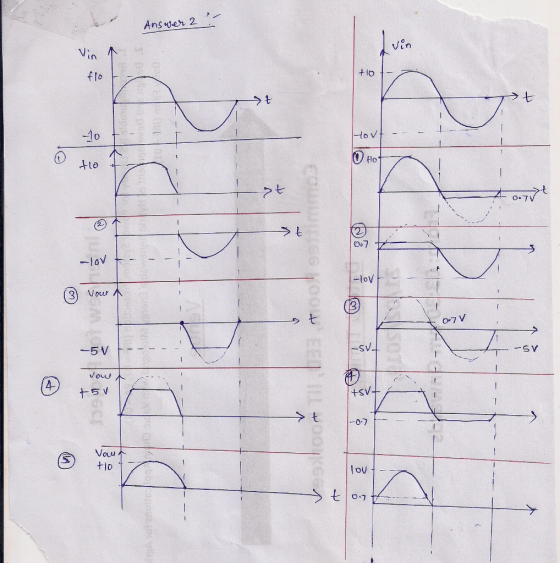
 For the double diode circuit shown in figure 2-1, answer the following questions. In Figure 2-1 a) (10pts) For the triangular wave input shown (Vin), sketch the output voltage (Vout) using the constant voltage drop model (CVD: Vo-0.7V). Be sure to note the voltage values on the y-axis of your Vout plot and show any equations you used to determine those values ime FEE 334: Spring 2019 Midterm b) (2pts) During the middle of the first time segment (when Vin...
Ctri Question 3 (20 Marks) Lab 1-Zener Circuits and Applications Theory: Zener diode is designed ...
 Ctri Question 3 (20 Marks) Lab 1-Zener Circuits and Applications Theory: Zener diode is designed to operate in reverse conduction. Zener breakdown occurs at a precisely defined voltage, allowing the diode to be used as a voltage reference or clipper. While Zener diodes are usually operated in reverse conduction, they may also be operated in cutoff and forward conduction. There are two different effects that are used in "Zener diodes". The only practical difference is that the two types have...
5. A light emitting diode (LED) is a diode that lights up when a current flows across it. The sym...
 5. A light emitting diode (LED) is a diode that lights up when a current flows across it. The symbol for an LED is shown below (sometimes wiggly arrows are used to represent the light instead.) For this question we will assume we are working with LEDs that have a turn-on voltage of VoN-1V and a reverse breakdown voltage of VBR-8V a. You hook up a single LED to a power supply that can put out vol tage from -10...
B. In each of the following circuits: [2 marks] Determine whether each silicon diode is forward...
 B. In each of the following circuits: [2 marks] Determine
whether each silicon diode is forward biased or reverse
biased
2 A vertical plate with a gap of 2.8 cm wide of infinite extent contains a fluid of viscosity 30 poise and specific gravity 0.8. A metallic plate 1.4 mx1.4 mx0.4 cm is to be lifted up with a constant velocity of 0.18 m/sec through the gap. If the plate is in the middle of the gap. Find the force...
B. In each of the following circuits: [2 marks] Determine
whether each silicon diode is forward biased or reverse
biased
2 A vertical plate with a gap of 2.8 cm wide of infinite extent contains a fluid of viscosity 30 poise and specific gravity 0.8. A metallic plate 1.4 mx1.4 mx0.4 cm is to be lifted up with a constant velocity of 0.18 m/sec through the gap. If the plate is in the middle of the gap. Find the force...
1. a) State the diode equation and explain the significance of each term. b) Sketch the current - voltage characteristics for a typical silicon diode over the 4 voltage range -2 V to +2 V. Explai...
 1. a) State the diode equation and explain the significance of each term. b) Sketch the current - voltage characteristics for a typical silicon diode over the 4 voltage range -2 V to +2 V. Explain how the characteristics would change if the diode was fabricated using germanium. Give an equivalent circuit representation of the device in each case. c) In a silicon diode a current of 200 HA flows when a forward bias voltage of 0.5 V4 is applied...
02 +Vo D3 Rgare 18 Circuit for Problem 1 Analysis 1. Copy the circuit of Figure 1.8 and sketch the ow of pesitive curment throughout the entire circuit for o>0. Repeat for n ce 2....
 02 +Vo D3 Rgare 18 Circuit for Problem 1 Analysis 1. Copy the circuit of Figure 1.8 and sketch the ow of pesitive curment throughout the entire circuit for o>0. Repeat for n ce 2. Plot two periods of nlt) and s) for each of the thee input wave shown in Figune 17 on page 37 fom output t (a) Feak value, and b) Eflective DC value, also known as RMS value NotTE These and are therefore optional 4. Determine...
A common source amplifier circuit based on a single n-channel MOSFET is shown in Figure 4b. Assume that the transconductance gm-60 mS (equivalent to mA/ V) and drain source resistance, os,...
 A common source amplifier circuit based on a single n-channel MOSFET is shown in Figure 4b. Assume that the transconductance gm-60 mS (equivalent to mA/ V) and drain source resistance, os, is so large it may be neglected. 0) Calculate the open circuit voltage gain Av Yout/ Vis. i) The amplifier has a load of 10 k2. Determine the current gain Va. = 12 V 150k 4k3 Vout Vin 200k GND = 0 V Figure 4b a) State the name...
 For the 4 circuits below, plot the V vs V, relationships (as demonstrated in Chapter 3) first without using EveryCircuit (EC) app Then build the circuits in EC, vary V, measure V, and plot V vs V. again based on the results obtained from EC app Assume V.-IV, R.-R. = 1kw and the diodes are ideal with Turn ON voltage of 0.7V (or OV meaning the diode is forward-biased and Di R and cathode terminal Circuit (a) ircuit (b) ircuit...
 (1) A simusoidal signal Vs is the input to the full-waverectifier shown. The diodes have a reverse saturation current 0.01 mA and an abrupt tum-on oltage of 0.7 V Theresistoris R-2,000 S2. Let Vs(t)- 12 cos(ot) V. D: D. D: D (a) Calculate the voltage Vo for the extremes of the sourc voltage,ie. VsMlax = 12 Vand (4 pts) (b)Calculate the source current for t-0 s, Vs(0)12 cos(ot) V. (6 pts) (b) Fill out the table showing when each diodeis...
 1) Assuming ideal op-amp characteristics, determine the gains (Vout/Vin) of the following amplifier circuits and the indicated currents. You should assume that voltage saturation is not a factor. U2 Vin=2= 11 15 2 Oy v Vout out 12 | 1k 14 Vin=2v — 111K OU Vout | thi I4 W 1 10k 110 U5115 OPAMP IZR1114 R13 Vout 3k R15 1116 ISVR12 3k 114 R16 113 R14 11k c) Vin = 4V
 For the double diode circuit shown in figure 2-1, answer the following questions. In Figure 2-1 a) (10pts) For the triangular wave input shown (Vin), sketch the output voltage (Vout) using the constant voltage drop model (CVD: Vo-0.7V). Be sure to note the voltage values on the y-axis of your Vout plot and show any equations you used to determine those values ime FEE 334: Spring 2019 Midterm b) (2pts) During the middle of the first time segment (when Vin...
 Ctri Question 3 (20 Marks) Lab 1-Zener Circuits and Applications Theory: Zener diode is designed to operate in reverse conduction. Zener breakdown occurs at a precisely defined voltage, allowing the diode to be used as a voltage reference or clipper. While Zener diodes are usually operated in reverse conduction, they may also be operated in cutoff and forward conduction. There are two different effects that are used in "Zener diodes". The only practical difference is that the two types have...
 5. A light emitting diode (LED) is a diode that lights up when a current flows across it. The symbol for an LED is shown below (sometimes wiggly arrows are used to represent the light instead.) For this question we will assume we are working with LEDs that have a turn-on voltage of VoN-1V and a reverse breakdown voltage of VBR-8V a. You hook up a single LED to a power supply that can put out vol tage from -10...
 B. In each of the following circuits: [2 marks] Determine
whether each silicon diode is forward biased or reverse
biased
2 A vertical plate with a gap of 2.8 cm wide of infinite extent contains a fluid of viscosity 30 poise and specific gravity 0.8. A metallic plate 1.4 mx1.4 mx0.4 cm is to be lifted up with a constant velocity of 0.18 m/sec through the gap. If the plate is in the middle of the gap. Find the force...
B. In each of the following circuits: [2 marks] Determine
whether each silicon diode is forward biased or reverse
biased
2 A vertical plate with a gap of 2.8 cm wide of infinite extent contains a fluid of viscosity 30 poise and specific gravity 0.8. A metallic plate 1.4 mx1.4 mx0.4 cm is to be lifted up with a constant velocity of 0.18 m/sec through the gap. If the plate is in the middle of the gap. Find the force...
 1. a) State the diode equation and explain the significance of each term. b) Sketch the current - voltage characteristics for a typical silicon diode over the 4 voltage range -2 V to +2 V. Explain how the characteristics would change if the diode was fabricated using germanium. Give an equivalent circuit representation of the device in each case. c) In a silicon diode a current of 200 HA flows when a forward bias voltage of 0.5 V4 is applied...
 02 +Vo D3 Rgare 18 Circuit for Problem 1 Analysis 1. Copy the circuit of Figure 1.8 and sketch the ow of pesitive curment throughout the entire circuit for o>0. Repeat for n ce 2. Plot two periods of nlt) and s) for each of the thee input wave shown in Figune 17 on page 37 fom output t (a) Feak value, and b) Eflective DC value, also known as RMS value NotTE These and are therefore optional 4. Determine...
 A common source amplifier circuit based on a single n-channel MOSFET is shown in Figure 4b. Assume that the transconductance gm-60 mS (equivalent to mA/ V) and drain source resistance, os, is so large it may be neglected. 0) Calculate the open circuit voltage gain Av Yout/ Vis. i) The amplifier has a load of 10 k2. Determine the current gain Va. = 12 V 150k 4k3 Vout Vin 200k GND = 0 V Figure 4b a) State the name...
Most questions answered within 3 hours.
-
An empty test tube weighs 15.923 grams. Then,
MgCl2•6H2O is added into the test tube. After...
asked 45 minutes ago -
Please answer true or false. Words
cannot be changed or added in to make it true...
asked 43 minutes ago -
(a) A piston at 6.1 atm contains a gas that occupies a volume of
3.5 L....
asked 44 minutes ago -
Assume memory access is 10 units of time and disk access is
10000 units of time....
asked 1 hour ago -
1. Are all good samples random?
2. Magazines often report surveys giving statistics such as “63%...
asked 1 hour ago -
Under all the various types of market structures, firms
must eventually earn some economic profits for...
asked 1 hour ago -
Consider the following fitness regime for a single locus trait
with two co-dominant alleles: w11 =...
asked 1 hour ago -
A large cable company reports the following.
80% of its customers subscribe to its cable TV...
asked 1 hour ago -
Please answer the question in brief.
Discuss the role of ERP in organizations. Are ERP tools...
asked 1 hour ago -
Discuss the pros and cons of collaborative software such
as SameTime. Does it increase productivity? What...
asked 1 hour ago -
Buying your in-laws a gift because it’s expected is
due to the ____________ motive of gift-giving....
asked 1 hour ago -
Calculate the expected value, the variance, and the standard
deviation of the given random variable X....
asked 2 hours ago