


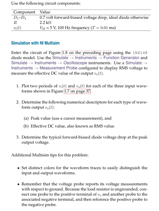
40 CHAPTER 1. DIODE CIRCUITS Use the following circuit components: Di-D 0.7 volt forward-biased voltage drop, ideal diode otherwise 2.2 kΩ VM-5 V, 100 Hz T- 0.01 ms) Simulation with NI Multisim Enter the circuit of Figure 1.8 on the preceding page using the 1N4148 diode model. Use the SimulateInstruments Function Generator and Simulate → Instruments → Oscilloscope instruments. Use a Simulate → Instruments-+ Measurement Probe configured to display RMS voltage to measure the effective DC value of the output o(t) 1. Plot two periods of n(t) and for each of the three input wave forms shown in Figure 1.7 on page 37 2. Determine the following numercal descriptors for each type of wave- form output o(): (a) Peak value (use a cursor measurement), and (b) Effective DC value, also known as RMS value 3. Determine the typical forward-biased diode voltage drop at the peak output voltage Additional Multisim tips for this problem: . Set distinct colors for the waveform traces to easily distinguish the input and output waveforms. . Remember that the voltage probe reports its voltage measurements with respect to ground. Because the load resistor is ungrounded, con- nect one probe to the positive terminal of o and another probe to the associated negative terminal, and then reference the positive probe to the negative probe
Figure1.8 shows a diode full-wave rectifier connected to a load resistance D1 D2 Vi + Vo - D3 D4 Figure 1.8: Circuit for Problem 1.8 Analysis 1. Copy the circuit of Figure 1.8 and sketch the flow of positive current throughout the entire circuit for vi> 0. Repeat for v
Homework Answers

Add Answer to:
02 +Vo D3 Rgare 18 Circuit for Problem 1 Analysis 1. Copy the circuit of Figure 1.8 and sketch the ow of pesitive curment throughout the entire circuit for o>0. Repeat for n ce 2....
nde) Figare 18 Circuit for Problem 15 Analysis 1. Plot the input and output vollage wavefoems nlt) and lt) as wel as the capacitor current iclt) for the input wavelorm shown in Fig ure 1....
 nde) Figare 18 Circuit for Problem 15 Analysis 1. Plot the input and output vollage wavefoems nlt) and lt) as wel as the capacitor current iclt) for the input wavelorm shown in Fig ure 1.10 on the next page, Assume the capacitoris initially discharged 2 Determine the following numerical descriptors for lf) and iclf (a) Voltage values of t) at times-250, 650, and 960ms. (b) Peak capacitor current t Discass the relationship between the plots of the capacitor current ic(t)...
please help Question 1 Consider the following circuit, where the reverse saturation current (Is) is the...
 please help
Question 1 Consider the following circuit, where the reverse saturation current (Is) is the same for each diode. D2 o Vo Di Vi WWW R 32 23 a. b. Determine an algebraic expression for V1, for a given Vo, and Is. Given an Is of 40 FA and R1 = 3.3 kl , determine the Vi that produces an output voltage (V.) of 0.625 V. C. Recalculate question-b if Is were to be a thousand times greater at...
please help
Question 1 Consider the following circuit, where the reverse saturation current (Is) is the same for each diode. D2 o Vo Di Vi WWW R 32 23 a. b. Determine an algebraic expression for V1, for a given Vo, and Is. Given an Is of 40 FA and R1 = 3.3 kl , determine the Vi that produces an output voltage (V.) of 0.625 V. C. Recalculate question-b if Is were to be a thousand times greater at...
For the double diode circuit shown in figure 2-1, answer the following questions. In Figure 2-1...
 For the double diode circuit shown in figure 2-1, answer the following questions. In Figure 2-1 a) (10pts) For the triangular wave input shown (Vin), sketch the output voltage (Vout) using the constant voltage drop model (CVD: Vo-0.7V). Be sure to note the voltage values on the y-axis of your Vout plot and show any equations you used to determine those values ime FEE 334: Spring 2019 Midterm b) (2pts) During the middle of the first time segment (when Vin...
Design a FULL WAVE BRIDGE RECTIFIER circuit that will: Take 120volts ac, 60 hz, sinusoidal waveform...
 Design a FULL WAVE BRIDGE RECTIFIER circuit that will:
Take 120volts ac, 60 hz, sinusoidal waveform and convert
it to a “regulated “dc value
giving 12 volts +, - 1 volt across a 2000-ohm output
load resistor with no more than 2%
ripple voltage.
You may assume:
a. An ideal power transformer as discussed in class.
b. For hand computations, you must assume a diode given by
Figure 4.8 page 185.
c. A filter capacitor sized per the textbook equation...
Design a FULL WAVE BRIDGE RECTIFIER circuit that will:
Take 120volts ac, 60 hz, sinusoidal waveform and convert
it to a “regulated “dc value
giving 12 volts +, - 1 volt across a 2000-ohm output
load resistor with no more than 2%
ripple voltage.
You may assume:
a. An ideal power transformer as discussed in class.
b. For hand computations, you must assume a diode given by
Figure 4.8 page 185.
c. A filter capacitor sized per the textbook equation...
A common source amplifier circuit based on a single n-channel MOSFET is shown in Figure 4b. Assume that the transconductance gm-60 mS (equivalent to mA/ V) and drain source resistance, os,...
 A common source amplifier circuit based on a single n-channel MOSFET is shown in Figure 4b. Assume that the transconductance gm-60 mS (equivalent to mA/ V) and drain source resistance, os, is so large it may be neglected. 0) Calculate the open circuit voltage gain Av Yout/ Vis. i) The amplifier has a load of 10 k2. Determine the current gain Va. = 12 V 150k 4k3 Vout Vin 200k GND = 0 V Figure 4b a) State the name...
Question 1: 7.33 +15V 1O MO R-200k 16n 7k MO 7.33 Figure P7.33 shows a discrete-circuit...
 Question 1: 7.33 +15V 1O MO R-200k 16n 7k MO 7.33 Figure P7.33 shows a discrete-circuit amplifier. The input signal is coupled to the gate through a very large capacitor (shown as infinite). The transistor source is connected to ground at signal frequencies via a very large capacitor (shown as infinite). The output voltage signal that develops at the drain is coupled to a load resistance via a very large capacitor (shown as infinite). All capacitors behave as short circuits...
Problem 3: Design Problem On Figure P3a, you have a Common Source (CS) n-channel MOSFET amplifier....
 Problem 3: Design Problem On Figure P3a, you have a Common Source (CS) n-channel MOSFET amplifier. Notice the absence of a source resistor Rsig and load resistor R. If we know how the present amplifier (the one on Figure P3a) behaves without Rsig and RL, we can infer its behaviors if Rsig and R were to be added. design the amplifier circuit on Figure P3a, i.e., you have to find appropriate values for RGj You are to RG,, RD, and...
 nde) Figare 18 Circuit for Problem 15 Analysis 1. Plot the input and output vollage wavefoems nlt) and lt) as wel as the capacitor current iclt) for the input wavelorm shown in Fig ure 1.10 on the next page, Assume the capacitoris initially discharged 2 Determine the following numerical descriptors for lf) and iclf (a) Voltage values of t) at times-250, 650, and 960ms. (b) Peak capacitor current t Discass the relationship between the plots of the capacitor current ic(t)...
 please help
Question 1 Consider the following circuit, where the reverse saturation current (Is) is the same for each diode. D2 o Vo Di Vi WWW R 32 23 a. b. Determine an algebraic expression for V1, for a given Vo, and Is. Given an Is of 40 FA and R1 = 3.3 kl , determine the Vi that produces an output voltage (V.) of 0.625 V. C. Recalculate question-b if Is were to be a thousand times greater at...
please help
Question 1 Consider the following circuit, where the reverse saturation current (Is) is the same for each diode. D2 o Vo Di Vi WWW R 32 23 a. b. Determine an algebraic expression for V1, for a given Vo, and Is. Given an Is of 40 FA and R1 = 3.3 kl , determine the Vi that produces an output voltage (V.) of 0.625 V. C. Recalculate question-b if Is were to be a thousand times greater at...
 For the double diode circuit shown in figure 2-1, answer the following questions. In Figure 2-1 a) (10pts) For the triangular wave input shown (Vin), sketch the output voltage (Vout) using the constant voltage drop model (CVD: Vo-0.7V). Be sure to note the voltage values on the y-axis of your Vout plot and show any equations you used to determine those values ime FEE 334: Spring 2019 Midterm b) (2pts) During the middle of the first time segment (when Vin...
 Design a FULL WAVE BRIDGE RECTIFIER circuit that will:
Take 120volts ac, 60 hz, sinusoidal waveform and convert
it to a “regulated “dc value
giving 12 volts +, - 1 volt across a 2000-ohm output
load resistor with no more than 2%
ripple voltage.
You may assume:
a. An ideal power transformer as discussed in class.
b. For hand computations, you must assume a diode given by
Figure 4.8 page 185.
c. A filter capacitor sized per the textbook equation...
Design a FULL WAVE BRIDGE RECTIFIER circuit that will:
Take 120volts ac, 60 hz, sinusoidal waveform and convert
it to a “regulated “dc value
giving 12 volts +, - 1 volt across a 2000-ohm output
load resistor with no more than 2%
ripple voltage.
You may assume:
a. An ideal power transformer as discussed in class.
b. For hand computations, you must assume a diode given by
Figure 4.8 page 185.
c. A filter capacitor sized per the textbook equation...
 A common source amplifier circuit based on a single n-channel MOSFET is shown in Figure 4b. Assume that the transconductance gm-60 mS (equivalent to mA/ V) and drain source resistance, os, is so large it may be neglected. 0) Calculate the open circuit voltage gain Av Yout/ Vis. i) The amplifier has a load of 10 k2. Determine the current gain Va. = 12 V 150k 4k3 Vout Vin 200k GND = 0 V Figure 4b a) State the name...
 Question 1: 7.33 +15V 1O MO R-200k 16n 7k MO 7.33 Figure P7.33 shows a discrete-circuit amplifier. The input signal is coupled to the gate through a very large capacitor (shown as infinite). The transistor source is connected to ground at signal frequencies via a very large capacitor (shown as infinite). The output voltage signal that develops at the drain is coupled to a load resistance via a very large capacitor (shown as infinite). All capacitors behave as short circuits...
 Problem 3: Design Problem On Figure P3a, you have a Common Source (CS) n-channel MOSFET amplifier. Notice the absence of a source resistor Rsig and load resistor R. If we know how the present amplifier (the one on Figure P3a) behaves without Rsig and RL, we can infer its behaviors if Rsig and R were to be added. design the amplifier circuit on Figure P3a, i.e., you have to find appropriate values for RGj You are to RG,, RD, and...
Most questions answered within 3 hours.
-
If authentic leadership is really a lifelong process,
can teenagers be authentic leaders? Why or why...
asked 1 minute ago -
Six years of quarterly data of a seasonally adjusted series are
used to estimate a linear...
asked 20 minutes ago -
Which of the following is not an ecological model used
to foster behavior change?
PRECEDE-PROCEED Model...
asked 23 minutes ago -
On the Apollo 14 mission to the moon, astronaut Alan Shepard hit
a golf ball with...
asked 19 minutes ago -
What are John’s potential claims if he is terminated
this week?
John is a 54-year-old man...
asked 33 minutes ago -
A (8.5) cm tall object is placed at a distance of (14.2) cm from
a convex...
asked 41 minutes ago -
(2) For the following questions, consider a data set that
exhibits a normal distribution. Report the...
asked 42 minutes ago -
What exactly is an information system? How does it work" What
are its people organization,
...
asked 44 minutes ago -
The Food Marketing Institute shows that 17% of households spend
more than $100 per week on...
asked 53 minutes ago -
Go to NCBI BLAST search web page
1st search: GEKDLRRAKDINQEVYNF
2nd search: PTSQRLQLLEPFDK
3rd search: GEKDLRRAKDINQEVYNF...
asked 57 minutes ago -
Explain how each of the following three conditions could be a
red flag for a register...
asked 1 hour ago -
In a two-way factorial ANOVA, the final F-ratio for
factor AxB is determined by dividing _____...
asked 1 hour ago