
Homework Answers


Add Answer to:
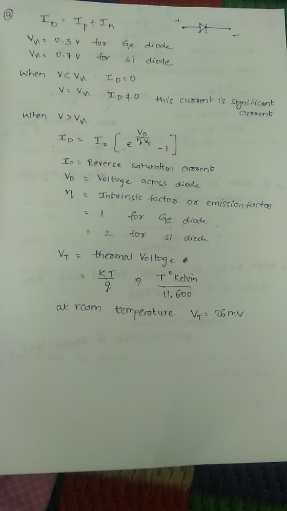
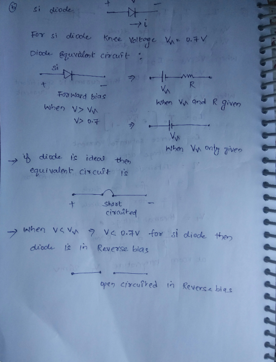
1. a) State the diode equation and explain the significance of each term. b) Sketch the current - voltage characteristics for a typical silicon diode over the 4 voltage range -2 V to +2 V. Explai...
1. at what voltage the current density in a p-n diode reaches a magnitude of 10 A/cm^2 ? the diode is made by doping with boron are phosphorous with concentrations of 10^18 and 10^19 cm^-3, respec...
 1. at what voltage the current density in a p-n diode
reaches a magnitude of 10 A/cm^2 ? the diode is made by doping with
boron are phosphorous with concentrations of 10^18 and 10^19 cm^-3,
respectively.
3. A MOSFET is made on silicon substrate doped with boron with a concentration of 10" cm. Width and length of channel are 100 and O.1 micron respectively. Thickness of the oxide insulator under the gate is 10 nm. Find transconductance of this transistor...
1. at what voltage the current density in a p-n diode
reaches a magnitude of 10 A/cm^2 ? the diode is made by doping with
boron are phosphorous with concentrations of 10^18 and 10^19 cm^-3,
respectively.
3. A MOSFET is made on silicon substrate doped with boron with a concentration of 10" cm. Width and length of channel are 100 and O.1 micron respectively. Thickness of the oxide insulator under the gate is 10 nm. Find transconductance of this transistor...
A common source amplifier circuit based on a single n-channel MOSFET is shown in Figure 4b. Assume that the transconductance gm-60 mS (equivalent to mA/ V) and drain source resistance, os,...
 A common source amplifier circuit based on a single n-channel MOSFET is shown in Figure 4b. Assume that the transconductance gm-60 mS (equivalent to mA/ V) and drain source resistance, os, is so large it may be neglected. 0) Calculate the open circuit voltage gain Av Yout/ Vis. i) The amplifier has a load of 10 k2. Determine the current gain Va. = 12 V 150k 4k3 Vout Vin 200k GND = 0 V Figure 4b a) State the name...
1. Consider a p*n silicon diode at T-300 K with doping concentrations of N 10 cin...
 1. Consider a p*n silicon diode at T-300 K with doping concentrations of N 10 cin and N-101 cm-3. The minority carier hole diffusion coefficient is D 12 cm2/s and the minority carrier hole lifetime is po 10-7 s. The cross sectional area is A 10- cm2. Calculate the reverse saturation current and the diode current at a forward-bias voltage of 0.50v A germanium p* n diode at T-300 K has the following parameters: Na 108 cm-3 N,--1016 cm", ,...
Problem 4: An abrupt silicon p-n junction diode has the following characteristics. side n-side N-4x 1016cm N1016cm3 n 1000 cm2/V sec 350 cm2/V sec Area A 102cm2 Calculate the following quantities...
 Problem 4: An abrupt silicon p-n junction diode has the following characteristics. side n-side N-4x 1016cm N1016cm3 n 1000 cm2/V sec 350 cm2/V sec Area A 102cm2 Calculate the following quantities: (a) Reverse saturation hole current component (b) Reverse saturation electron current component. (c) Minority carrier concentrations at the edge of the depletion layer, p(0) and pr(0), for a forward voltage of 0.6 V (d) Electron and hole current for the bias condition of (c). (e) Make a rough sketch...
Qno2 only HOME INSERT DESIGN PAGE LAYOUT REFERENCES MAILINGS REVIEW VIEW LE Alexander Zaitsev Final Test ENS345, Spring 2019 1. At a forward voltage of 2 V, the current density in a symmetric p-n dio...
 Qno2 only
HOME INSERT DESIGN PAGE LAYOUT REFERENCES MAILINGS REVIEW VIEW LE Alexander Zaitsev Final Test ENS345, Spring 2019 1. At a forward voltage of 2 V, the current density in a symmetric p-n diode is 10A/cm2. Estimate concentration of doping in this diode. 2. A silicon BIT with De = 10 cm2/s, DF 40 cm2/s, We = 100 nm, wa-50 nm, Na = 1017 crm-3, NE-1020cm -3 has a 0.99. Estimate bandgap width of the base of this transistor....
Qno2 only
HOME INSERT DESIGN PAGE LAYOUT REFERENCES MAILINGS REVIEW VIEW LE Alexander Zaitsev Final Test ENS345, Spring 2019 1. At a forward voltage of 2 V, the current density in a symmetric p-n diode is 10A/cm2. Estimate concentration of doping in this diode. 2. A silicon BIT with De = 10 cm2/s, DF 40 cm2/s, We = 100 nm, wa-50 nm, Na = 1017 crm-3, NE-1020cm -3 has a 0.99. Estimate bandgap width of the base of this transistor....
Explain the answer 1. Consider the following MOSFET characteristics. What type of device is it? A....
 Explain the answer
1. Consider the following MOSFET characteristics. What type of device is it? A. N-channel depletion-mode MOSFET B. N-channel enhancement-mode MOSFET. C. P-channel depletion-mode MOSFET. D. P-channel enhancement-mode MOSFET. Ip(mA) 1.5 1.0 0.5 V 00 V 0 0 2.0 4.0 6.0 Consider an n-channel MOSFET. Assuming no interface charge due to defects and/or traps, how would the the following parameters change when the oxide thickness is reduced? The flat band voltage VFB A. Increase B. Increase; c. Unchange:...
Explain the answer
1. Consider the following MOSFET characteristics. What type of device is it? A. N-channel depletion-mode MOSFET B. N-channel enhancement-mode MOSFET. C. P-channel depletion-mode MOSFET. D. P-channel enhancement-mode MOSFET. Ip(mA) 1.5 1.0 0.5 V 00 V 0 0 2.0 4.0 6.0 Consider an n-channel MOSFET. Assuming no interface charge due to defects and/or traps, how would the the following parameters change when the oxide thickness is reduced? The flat band voltage VFB A. Increase B. Increase; c. Unchange:...
Qno3 only use formulaes as given in question Final Test EN$345, Spring 2019 1. At what voltagethe current density in a p n diode reaches doping with boron are phosphorous with concent a magnitude...
 Qno3 only
use formulaes as given in question
Final Test EN$345, Spring 2019 1. At what voltagethe current density in a p n diode reaches doping with boron are phosphorous with concent a magnitude of 10V/cm2? The diode is made by concentrations of 10 and 10cm 2. Assume the following parameters for a silicon BT: D. 10 cma a-40 cm'/s, w,-100 nm, W: 50 nm, -101, crn",N-10 ocm? . Base is made of a Sase alloy witafa-80 mev. Find β...
Qno3 only
use formulaes as given in question
Final Test EN$345, Spring 2019 1. At what voltagethe current density in a p n diode reaches doping with boron are phosphorous with concent a magnitude of 10V/cm2? The diode is made by concentrations of 10 and 10cm 2. Assume the following parameters for a silicon BT: D. 10 cma a-40 cm'/s, w,-100 nm, W: 50 nm, -101, crn",N-10 ocm? . Base is made of a Sase alloy witafa-80 mev. Find β...
1) Briefly explain the difference between the I-V relationships of a silicon and a gallium arsenide PN diode. 2) A certain semiconductor has energy gap of 2.48eV. Determine the range of wavelength...
 1) Briefly explain the difference between the I-V relationships of a silicon and a gallium arsenide PN diode. 2) A certain semiconductor has energy gap of 2.48eV. Determine the range of wavelengths that are absorbed by the semiconductor 21 Why is the collector current in a PNP transistor in the inverse active region much smaller than in the active region?
1) Briefly explain the difference between the I-V relationships of a silicon and a gallium arsenide PN diode. 2) A...
1) Briefly explain the difference between the I-V relationships of a silicon and a gallium arsenide PN diode. 2) A certain semiconductor has energy gap of 2.48eV. Determine the range of wavelengths that are absorbed by the semiconductor 21 Why is the collector current in a PNP transistor in the inverse active region much smaller than in the active region?
1) Briefly explain the difference between the I-V relationships of a silicon and a gallium arsenide PN diode. 2) A...
all please TEST #3 of the FET and are unaffected by 1. Schokley's equation defines the...
 all please
TEST #3 of the FET and are unaffected by 1. Schokley's equation defines the the network in which the device is employed. (a) Vas characteristics (b) drain characteristics (c) input output characteristics (d) transfer characteristics 2. For an N-channel JFET Ipss -8 mA and Vp-6 V. If Vas-2 V then what is the value of the drain current ID? (a) 2.666 mA (b) 3.5 LA (c) 3.55 mA (d) 5.33 mA 3. D-MOSFETs can operate in: (a) The...
all please
TEST #3 of the FET and are unaffected by 1. Schokley's equation defines the the network in which the device is employed. (a) Vas characteristics (b) drain characteristics (c) input output characteristics (d) transfer characteristics 2. For an N-channel JFET Ipss -8 mA and Vp-6 V. If Vas-2 V then what is the value of the drain current ID? (a) 2.666 mA (b) 3.5 LA (c) 3.55 mA (d) 5.33 mA 3. D-MOSFETs can operate in: (a) The...
Thanks.... Question 2 (5 marks) a) State the ideal-diode equation. b) Forward-bias-voltage of V, 0.625 V...
 Thanks....
Question 2 (5 marks) a) State the ideal-diode equation. b) Forward-bias-voltage of V, 0.625 V is applied to a silicon p-n junction with its cross 10 cm2. At T 300 K, it has the following parameters: n, 1.5 x 100 cm3 N, 5 x 1016 cm3 Na-1 x 106 cm D, 25 cm'ls D, 10 cm/s Tao 5 x 10s tpo 1 x 10s sectional area, A Calculate: i) the minority electron diffusion current at the space charge edge,...
Thanks....
Question 2 (5 marks) a) State the ideal-diode equation. b) Forward-bias-voltage of V, 0.625 V is applied to a silicon p-n junction with its cross 10 cm2. At T 300 K, it has the following parameters: n, 1.5 x 100 cm3 N, 5 x 1016 cm3 Na-1 x 106 cm D, 25 cm'ls D, 10 cm/s Tao 5 x 10s tpo 1 x 10s sectional area, A Calculate: i) the minority electron diffusion current at the space charge edge,...
 1. at what voltage the current density in a p-n diode
reaches a magnitude of 10 A/cm^2 ? the diode is made by doping with
boron are phosphorous with concentrations of 10^18 and 10^19 cm^-3,
respectively.
3. A MOSFET is made on silicon substrate doped with boron with a concentration of 10" cm. Width and length of channel are 100 and O.1 micron respectively. Thickness of the oxide insulator under the gate is 10 nm. Find transconductance of this transistor...
1. at what voltage the current density in a p-n diode
reaches a magnitude of 10 A/cm^2 ? the diode is made by doping with
boron are phosphorous with concentrations of 10^18 and 10^19 cm^-3,
respectively.
3. A MOSFET is made on silicon substrate doped with boron with a concentration of 10" cm. Width and length of channel are 100 and O.1 micron respectively. Thickness of the oxide insulator under the gate is 10 nm. Find transconductance of this transistor...
 A common source amplifier circuit based on a single n-channel MOSFET is shown in Figure 4b. Assume that the transconductance gm-60 mS (equivalent to mA/ V) and drain source resistance, os, is so large it may be neglected. 0) Calculate the open circuit voltage gain Av Yout/ Vis. i) The amplifier has a load of 10 k2. Determine the current gain Va. = 12 V 150k 4k3 Vout Vin 200k GND = 0 V Figure 4b a) State the name...
 1. Consider a p*n silicon diode at T-300 K with doping concentrations of N 10 cin and N-101 cm-3. The minority carier hole diffusion coefficient is D 12 cm2/s and the minority carrier hole lifetime is po 10-7 s. The cross sectional area is A 10- cm2. Calculate the reverse saturation current and the diode current at a forward-bias voltage of 0.50v A germanium p* n diode at T-300 K has the following parameters: Na 108 cm-3 N,--1016 cm", ,...
 Problem 4: An abrupt silicon p-n junction diode has the following characteristics. side n-side N-4x 1016cm N1016cm3 n 1000 cm2/V sec 350 cm2/V sec Area A 102cm2 Calculate the following quantities: (a) Reverse saturation hole current component (b) Reverse saturation electron current component. (c) Minority carrier concentrations at the edge of the depletion layer, p(0) and pr(0), for a forward voltage of 0.6 V (d) Electron and hole current for the bias condition of (c). (e) Make a rough sketch...
 Qno2 only
HOME INSERT DESIGN PAGE LAYOUT REFERENCES MAILINGS REVIEW VIEW LE Alexander Zaitsev Final Test ENS345, Spring 2019 1. At a forward voltage of 2 V, the current density in a symmetric p-n diode is 10A/cm2. Estimate concentration of doping in this diode. 2. A silicon BIT with De = 10 cm2/s, DF 40 cm2/s, We = 100 nm, wa-50 nm, Na = 1017 crm-3, NE-1020cm -3 has a 0.99. Estimate bandgap width of the base of this transistor....
Qno2 only
HOME INSERT DESIGN PAGE LAYOUT REFERENCES MAILINGS REVIEW VIEW LE Alexander Zaitsev Final Test ENS345, Spring 2019 1. At a forward voltage of 2 V, the current density in a symmetric p-n diode is 10A/cm2. Estimate concentration of doping in this diode. 2. A silicon BIT with De = 10 cm2/s, DF 40 cm2/s, We = 100 nm, wa-50 nm, Na = 1017 crm-3, NE-1020cm -3 has a 0.99. Estimate bandgap width of the base of this transistor....
 Explain the answer
1. Consider the following MOSFET characteristics. What type of device is it? A. N-channel depletion-mode MOSFET B. N-channel enhancement-mode MOSFET. C. P-channel depletion-mode MOSFET. D. P-channel enhancement-mode MOSFET. Ip(mA) 1.5 1.0 0.5 V 00 V 0 0 2.0 4.0 6.0 Consider an n-channel MOSFET. Assuming no interface charge due to defects and/or traps, how would the the following parameters change when the oxide thickness is reduced? The flat band voltage VFB A. Increase B. Increase; c. Unchange:...
Explain the answer
1. Consider the following MOSFET characteristics. What type of device is it? A. N-channel depletion-mode MOSFET B. N-channel enhancement-mode MOSFET. C. P-channel depletion-mode MOSFET. D. P-channel enhancement-mode MOSFET. Ip(mA) 1.5 1.0 0.5 V 00 V 0 0 2.0 4.0 6.0 Consider an n-channel MOSFET. Assuming no interface charge due to defects and/or traps, how would the the following parameters change when the oxide thickness is reduced? The flat band voltage VFB A. Increase B. Increase; c. Unchange:...
 Qno3 only
use formulaes as given in question
Final Test EN$345, Spring 2019 1. At what voltagethe current density in a p n diode reaches doping with boron are phosphorous with concent a magnitude of 10V/cm2? The diode is made by concentrations of 10 and 10cm 2. Assume the following parameters for a silicon BT: D. 10 cma a-40 cm'/s, w,-100 nm, W: 50 nm, -101, crn",N-10 ocm? . Base is made of a Sase alloy witafa-80 mev. Find β...
Qno3 only
use formulaes as given in question
Final Test EN$345, Spring 2019 1. At what voltagethe current density in a p n diode reaches doping with boron are phosphorous with concent a magnitude of 10V/cm2? The diode is made by concentrations of 10 and 10cm 2. Assume the following parameters for a silicon BT: D. 10 cma a-40 cm'/s, w,-100 nm, W: 50 nm, -101, crn",N-10 ocm? . Base is made of a Sase alloy witafa-80 mev. Find β...
 1) Briefly explain the difference between the I-V relationships of a silicon and a gallium arsenide PN diode. 2) A certain semiconductor has energy gap of 2.48eV. Determine the range of wavelengths that are absorbed by the semiconductor 21 Why is the collector current in a PNP transistor in the inverse active region much smaller than in the active region?
1) Briefly explain the difference between the I-V relationships of a silicon and a gallium arsenide PN diode. 2) A...
1) Briefly explain the difference between the I-V relationships of a silicon and a gallium arsenide PN diode. 2) A certain semiconductor has energy gap of 2.48eV. Determine the range of wavelengths that are absorbed by the semiconductor 21 Why is the collector current in a PNP transistor in the inverse active region much smaller than in the active region?
1) Briefly explain the difference between the I-V relationships of a silicon and a gallium arsenide PN diode. 2) A...
 all please
TEST #3 of the FET and are unaffected by 1. Schokley's equation defines the the network in which the device is employed. (a) Vas characteristics (b) drain characteristics (c) input output characteristics (d) transfer characteristics 2. For an N-channel JFET Ipss -8 mA and Vp-6 V. If Vas-2 V then what is the value of the drain current ID? (a) 2.666 mA (b) 3.5 LA (c) 3.55 mA (d) 5.33 mA 3. D-MOSFETs can operate in: (a) The...
all please
TEST #3 of the FET and are unaffected by 1. Schokley's equation defines the the network in which the device is employed. (a) Vas characteristics (b) drain characteristics (c) input output characteristics (d) transfer characteristics 2. For an N-channel JFET Ipss -8 mA and Vp-6 V. If Vas-2 V then what is the value of the drain current ID? (a) 2.666 mA (b) 3.5 LA (c) 3.55 mA (d) 5.33 mA 3. D-MOSFETs can operate in: (a) The...
 Thanks....
Question 2 (5 marks) a) State the ideal-diode equation. b) Forward-bias-voltage of V, 0.625 V is applied to a silicon p-n junction with its cross 10 cm2. At T 300 K, it has the following parameters: n, 1.5 x 100 cm3 N, 5 x 1016 cm3 Na-1 x 106 cm D, 25 cm'ls D, 10 cm/s Tao 5 x 10s tpo 1 x 10s sectional area, A Calculate: i) the minority electron diffusion current at the space charge edge,...
Thanks....
Question 2 (5 marks) a) State the ideal-diode equation. b) Forward-bias-voltage of V, 0.625 V is applied to a silicon p-n junction with its cross 10 cm2. At T 300 K, it has the following parameters: n, 1.5 x 100 cm3 N, 5 x 1016 cm3 Na-1 x 106 cm D, 25 cm'ls D, 10 cm/s Tao 5 x 10s tpo 1 x 10s sectional area, A Calculate: i) the minority electron diffusion current at the space charge edge,...
Most questions answered within 3 hours.
-
Remember: Changes in supply determinants shift supply, and
changes in demand determinants shift demand. We say...
asked 34 seconds ago -
A football with a mass of 1.2 kg is kicked from ground level to
a height...
asked 1 minute ago -
Why is the answer b), for this question? I came up with C) for
my incorrect...
asked 6 minutes ago -
Suppose that you know that in the population of full-time
employees in the United States, the...
asked 28 minutes ago -
This experiment was designed originally to sample various meat and carcass quality
aspects of Ontario pigs...
asked 29 minutes ago -
Dopamine Hydrochloride: draw the structure And Show the
functional groups in different colors and label the...
asked 21 minutes ago -
A rope supports a 10 kg dumbbell hanging from it. What is the
tension in the...
asked 20 minutes ago -
) Raw materials are studied for contamination. Suppose that
the number of particles of contamination per...
asked 43 minutes ago -
After running a regression analysis we calculated an F test and
the significance level was 0.15....
asked 39 minutes ago -
----Can someone please help me solve this one using JAVA
----I thank you in advance
Create...
asked 43 minutes ago -
1. What force primarily attracts the potassium ion to
the nitrate ion?
a. London forces...
asked 45 minutes ago -
What are the negative effects of abruptly stopping the use of
all fossil fuels? Give at...
asked 52 minutes ago