
Homework Answers
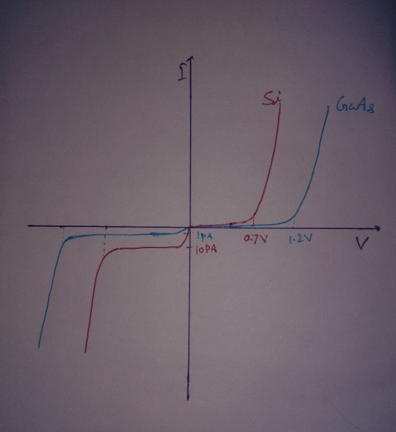
1.) I-V characteristics curves of both Si and GaAs based P-N diodes have nearly same nature. The difference between their I-V characteristics are-
- In Forward region, cut-in potential or barrier height for both p-n junctions are different. It is Vb= 0.7 V for Si based p-n junction while for GaAs based p-n junction Vb=1.2 V.
- In reverse region, GaAs based p-n diode has less reverse saturation current (Is= 1pA Approx.) than Si based p-n diode (is= 10pA Approx.). And in case of Si based p-n diode reverse breakdown earlier than that of GaAs based p-n diode as shown in figure.
2.) Energy band gap Eg=2.48 eV.
photons with energy less than the band gap energy will pass though the semiconductor while photons with energy greater than band gap energy are absorbed.
The wavelength of photons that can be absorbed by semiconductor can be determined as


Thus photons with wavelength less than 
3.)In active region of PNP transistor the emitter-base region is forward biased, while the collector-base junction is reverse biased so holes are injected into the base. The base is very thin, and most of the holes cross the reverse-biased base–collector junction and to be collected at the collector.So collector current is mainly due to the injection of holes from heavily doped emitter.

where 
But in case of inverse active region E-B junction is reverse biased, so minority charge carriers i.e. electrons will be injected into base ,since base is very thin so electrons are now collected at collectors. Here collector current is due to minority charge carriers of heavily doped emitter so this current must bs less than the current in cace of active region.
Add Answer to:
1) Briefly explain the difference between the I-V relationships of a silicon and a gallium arsenide PN diode. 2) A certain semiconductor has energy gap of 2.48eV. Determine the range of wavelength...
1) Briefly explain the difference between the I-V relationships of a silicon and a gallium arsenide...
 1) Briefly explain the difference between the I-V relationships of a silicon and a gallium arsenide PN diode. 2) A certain semiconductor has energy gap of 2.48eV. Determine the range of wavelengths that are absorbed by the semiconductor 21 Why is the collector current in a PNP transistor in the inverse active region much smaller than in the active region?
1. a) State the diode equation and explain the significance of each term. b) Sketch the current - voltage characteristics for a typical silicon diode over the 4 voltage range -2 V to +2 V. Explai...
 1. a) State the diode equation and explain the significance of each term. b) Sketch the current - voltage characteristics for a typical silicon diode over the 4 voltage range -2 V to +2 V. Explain how the characteristics would change if the diode was fabricated using germanium. Give an equivalent circuit representation of the device in each case. c) In a silicon diode a current of 200 HA flows when a forward bias voltage of 0.5 V4 is applied...
 1) Briefly explain the difference between the I-V relationships of a silicon and a gallium arsenide PN diode. 2) A certain semiconductor has energy gap of 2.48eV. Determine the range of wavelengths that are absorbed by the semiconductor 21 Why is the collector current in a PNP transistor in the inverse active region much smaller than in the active region?
 1. a) State the diode equation and explain the significance of each term. b) Sketch the current - voltage characteristics for a typical silicon diode over the 4 voltage range -2 V to +2 V. Explain how the characteristics would change if the diode was fabricated using germanium. Give an equivalent circuit representation of the device in each case. c) In a silicon diode a current of 200 HA flows when a forward bias voltage of 0.5 V4 is applied...
Most questions answered within 3 hours.
-
Question no 2
A housekeeping support department budgets its costs at
SR 40,000 per month plus...
asked 1 minute ago -
What is the pressure inside a 33.0 L container holding 106.4 kg
of argon gas at...
asked 5 minutes ago -
A 1400Kg sports car accelerates from rest to 90km/h in 7.0s.
What is the average power...
asked 42 minutes ago -
For the following reaction, 0.128 moles of
potassium hydrogen sulfateare mixed with
0.504 moles of potassium...
asked 4 hours ago -
1. What is the present value of $400, three years in the future
if the interest...
asked 4 hours ago -
The labor force minus the number of employed equals the number
of unemployed.
a. True
b....
asked 6 hours ago -
Determine the mass in units of grams [g] of 0.49 moles [mol]
of a new fictitious...
asked 7 hours ago -
A horizontal mass of M=5kg is on a spring and stretched to
x=0.5m when released from...
asked 8 hours ago -
26 of 50
"I have worked at the Arizona Humane Society for ten years, and
have...
asked 8 hours ago -
Compare and contrast zero based budgeting and incremental (or
base year) budgeting.
asked 8 hours ago -
4 pts 10. Which of the following hypothesis would be MOST
difficult to test experimentally? Group...
asked 8 hours ago -
A business owner makes 1,000 items a day. Each day he or she
contributes eight hours...
asked 8 hours ago