
Homework Answers


Add Answer to:
all please
TEST #3 of the FET and are unaffected by 1. Schokley's equation defines the...
Explain the answer 1. Consider the following MOSFET characteristics. What type of device is it? A....
 Explain the answer
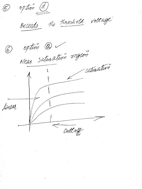
1. Consider the following MOSFET characteristics. What type of device is it? A. N-channel depletion-mode MOSFET B. N-channel enhancement-mode MOSFET. C. P-channel depletion-mode MOSFET. D. P-channel enhancement-mode MOSFET. Ip(mA) 1.5 1.0 0.5 V 00 V 0 0 2.0 4.0 6.0 Consider an n-channel MOSFET. Assuming no interface charge due to defects and/or traps, how would the the following parameters change when the oxide thickness is reduced? The flat band voltage VFB A. Increase B. Increase; c. Unchange:...
Explain the answer
1. Consider the following MOSFET characteristics. What type of device is it? A. N-channel depletion-mode MOSFET B. N-channel enhancement-mode MOSFET. C. P-channel depletion-mode MOSFET. D. P-channel enhancement-mode MOSFET. Ip(mA) 1.5 1.0 0.5 V 00 V 0 0 2.0 4.0 6.0 Consider an n-channel MOSFET. Assuming no interface charge due to defects and/or traps, how would the the following parameters change when the oxide thickness is reduced? The flat band voltage VFB A. Increase B. Increase; c. Unchange:...
MULTIPLE CHOICE. Choose the one alternative that best completes the statement or answers the question. 1)...
 MULTIPLE CHOICE. Choose the one alternative that best completes the statement or answers the question. 1) The maximum current in a JFET is defined as loss and occurs when VGS is equal to 1) A) zero Volts B) pinch-off voltage C) a voltage greater than the pinch-off voltage D) a small positive voltage of the FET and are unaffected by the network in which 2) 2) Schokley's equation defines the the device is employed. A) transfer characteristics C) drain characteristics...
Please show 18-33 clearly i am having a hard time understanding the graphing method. i understand...
 please show 18-33 clearly i am having a hard time
understanding the graphing method. i understand shockleys equation
fine
Vertical Sens 1 MA per dn i V per dav 45mA 500 mV Fas-15V per dav I V drv Figure 3.21 Drain charactenstics for a 2N4416 JTET transislor as displayed on a 18. Using the characteristics of Fig. 5.21 21. Using Ipss 9 mA and Vp3 V for the characteristics of Fig. 5.21, calculate Ip at Vos 1 V using Shockley's...
please show 18-33 clearly i am having a hard time
understanding the graphing method. i understand shockleys equation
fine
Vertical Sens 1 MA per dn i V per dav 45mA 500 mV Fas-15V per dav I V drv Figure 3.21 Drain charactenstics for a 2N4416 JTET transislor as displayed on a 18. Using the characteristics of Fig. 5.21 21. Using Ipss 9 mA and Vp3 V for the characteristics of Fig. 5.21, calculate Ip at Vos 1 V using Shockley's...
can you solve these questions ? 7,12,16,18,19 TULIS U, and 8 from eBook : pages 441-44x,...
 can you solve these questions ? 7,12,16,18,19
TULIS U, and 8 from eBook : pages 441-44x, pages 474-475 and pages 538-539 Solve the following problem: 7. A certain JFET datasheet gives VGS(of) = -8 V and Ipss = 10 mA. When VGS = 0, what is Ip for values of Vps above pinch off? Vpp = 15 V. 12. For a particular JFET. Smo = 3200 us. What is gm when Vos = -4V, given that VGs(off) = -8 V?...
can you solve these questions ? 7,12,16,18,19
TULIS U, and 8 from eBook : pages 441-44x, pages 474-475 and pages 538-539 Solve the following problem: 7. A certain JFET datasheet gives VGS(of) = -8 V and Ipss = 10 mA. When VGS = 0, what is Ip for values of Vps above pinch off? Vpp = 15 V. 12. For a particular JFET. Smo = 3200 us. What is gm when Vos = -4V, given that VGs(off) = -8 V?...
the Ebers-Moll VT = kB T/e. (c) Use your result from part (b) to find the...
 the Ebers-Moll VT = kB T/e. (c) Use your result from part (b) to find the resistance Rg necessary to generate 7.5μΑ of current with 20μΑ of programming current. (programming 6. FET I-V Curves. [10 pts.] Consider the family of I- V curves for a field effect transistor (FET) shown below. (a) Are the curves shown for a JFET or or an en- hancement mode MOSFET? Explain briefly how you know. (b) Table values for the given gain-source volt- ages...
ANSWER ALL QUESTIONS: 0-1. Study the circuit diagram given in Figurel and answer the following questions....
 ANSWER ALL QUESTIONS: 0-1. Study the circuit diagram given in Figurel and answer the following questions. (1.5 marks) i.) When the square wave voltage is + 5V, the transistor will be in which region? c) Saturation ii.) When the square wave voltage is OV, the transistor will be in which region? a) Cutoff region b) Saturation c) Active region iii.) When transistor operates in Saturation region, what are the values of Vce, and Ic? iv.) When transistor operates in Cutoff...
2. Consider an N-channel MOSFET circuit where the gate and drain terminals are shorted to- gether...
 Please help, and explain as much as possible. Thank
you!
2. Consider an N-channel MOSFET circuit where the gate and drain terminals are shorted to- gether2 as shown in Figre 2. Assume that the MOSFET has trans-conductance parameter of gm = 0.5mA/V and the threshold voltage of 0.7V (a) Identify in which region the n-channel MOSFET is operating (Triode region or Saturation region)? (b) Write MATLAB code to compute the drain current for the following gate-to-source voltage, Vcs Ves-VDs 0,1,2,3,4,5,6,7...
Please help, and explain as much as possible. Thank
you!
2. Consider an N-channel MOSFET circuit where the gate and drain terminals are shorted to- gether2 as shown in Figre 2. Assume that the MOSFET has trans-conductance parameter of gm = 0.5mA/V and the threshold voltage of 0.7V (a) Identify in which region the n-channel MOSFET is operating (Triode region or Saturation region)? (b) Write MATLAB code to compute the drain current for the following gate-to-source voltage, Vcs Ves-VDs 0,1,2,3,4,5,6,7...
December 2013 Elec-B5, Advanced Electronics QUESTION (1) In the following circuits, assume all transistors have the following parameters: K 0.5 mA/V2, VT,-1 V and λ-0.02. Given: 1M bias I mA M M2...
 December 2013 Elec-B5, Advanced Electronics QUESTION (1) In the following circuits, assume all transistors have the following parameters: K 0.5 mA/V2, VT,-1 V and λ-0.02. Given: 1M bias I mA M M2 꼬 + 2 고 (~ 2 a) Estimate the differential gain vourlVIN in (V/V) b) Find the common mode input resistance Ricm c) Find the common mode input range. d) Estimate the common mode rejection ratio, CMRR. Express your result in dB. Useful formulae: for n-channel MOSFET (6...
5). In this problem, you are asked to consider the ac hybrid-x model for an NMOS transistor and t...
 5). In this problem, you are asked to consider the ac hybrid-x model for an NMOS transistor and to relate the capacitors to the physical device structure. Recall the oxide capacitance per unit area ox) appears in the DC Ip-Vs relationship for triode and saturation regions. The NMOS transistor has kn-0.2 mA/V2, W 10 μm, L-I μm and μ,-1000 cm2/Vsec. a) Find the total gate-to-channel capacitance for small VDs, CG-cho. Hint: this is the parallel-plate capacitance between the gate and...
Q1 Which of the following is true for a MOS capacitor with a P-type body? Select...
Q1 Which of the following is true for a MOS capacitor with a P-type body? Select one: a. The charge in the inversion layer stays approximately constant as the gate voltage is increased above the threshold voltage b. The charge in the depletion region is proportional to the square root of the depletion region width, assuming that the body is uniformly doped c. In inversion, the total charge is equal to the sum of the charge in the depletion region...
 Explain the answer
1. Consider the following MOSFET characteristics. What type of device is it? A. N-channel depletion-mode MOSFET B. N-channel enhancement-mode MOSFET. C. P-channel depletion-mode MOSFET. D. P-channel enhancement-mode MOSFET. Ip(mA) 1.5 1.0 0.5 V 00 V 0 0 2.0 4.0 6.0 Consider an n-channel MOSFET. Assuming no interface charge due to defects and/or traps, how would the the following parameters change when the oxide thickness is reduced? The flat band voltage VFB A. Increase B. Increase; c. Unchange:...
Explain the answer
1. Consider the following MOSFET characteristics. What type of device is it? A. N-channel depletion-mode MOSFET B. N-channel enhancement-mode MOSFET. C. P-channel depletion-mode MOSFET. D. P-channel enhancement-mode MOSFET. Ip(mA) 1.5 1.0 0.5 V 00 V 0 0 2.0 4.0 6.0 Consider an n-channel MOSFET. Assuming no interface charge due to defects and/or traps, how would the the following parameters change when the oxide thickness is reduced? The flat band voltage VFB A. Increase B. Increase; c. Unchange:...
 MULTIPLE CHOICE. Choose the one alternative that best completes the statement or answers the question. 1) The maximum current in a JFET is defined as loss and occurs when VGS is equal to 1) A) zero Volts B) pinch-off voltage C) a voltage greater than the pinch-off voltage D) a small positive voltage of the FET and are unaffected by the network in which 2) 2) Schokley's equation defines the the device is employed. A) transfer characteristics C) drain characteristics...
 please show 18-33 clearly i am having a hard time
understanding the graphing method. i understand shockleys equation
fine
Vertical Sens 1 MA per dn i V per dav 45mA 500 mV Fas-15V per dav I V drv Figure 3.21 Drain charactenstics for a 2N4416 JTET transislor as displayed on a 18. Using the characteristics of Fig. 5.21 21. Using Ipss 9 mA and Vp3 V for the characteristics of Fig. 5.21, calculate Ip at Vos 1 V using Shockley's...
please show 18-33 clearly i am having a hard time
understanding the graphing method. i understand shockleys equation
fine
Vertical Sens 1 MA per dn i V per dav 45mA 500 mV Fas-15V per dav I V drv Figure 3.21 Drain charactenstics for a 2N4416 JTET transislor as displayed on a 18. Using the characteristics of Fig. 5.21 21. Using Ipss 9 mA and Vp3 V for the characteristics of Fig. 5.21, calculate Ip at Vos 1 V using Shockley's...
 can you solve these questions ? 7,12,16,18,19
TULIS U, and 8 from eBook : pages 441-44x, pages 474-475 and pages 538-539 Solve the following problem: 7. A certain JFET datasheet gives VGS(of) = -8 V and Ipss = 10 mA. When VGS = 0, what is Ip for values of Vps above pinch off? Vpp = 15 V. 12. For a particular JFET. Smo = 3200 us. What is gm when Vos = -4V, given that VGs(off) = -8 V?...
can you solve these questions ? 7,12,16,18,19
TULIS U, and 8 from eBook : pages 441-44x, pages 474-475 and pages 538-539 Solve the following problem: 7. A certain JFET datasheet gives VGS(of) = -8 V and Ipss = 10 mA. When VGS = 0, what is Ip for values of Vps above pinch off? Vpp = 15 V. 12. For a particular JFET. Smo = 3200 us. What is gm when Vos = -4V, given that VGs(off) = -8 V?...
 the Ebers-Moll VT = kB T/e. (c) Use your result from part (b) to find the resistance Rg necessary to generate 7.5μΑ of current with 20μΑ of programming current. (programming 6. FET I-V Curves. [10 pts.] Consider the family of I- V curves for a field effect transistor (FET) shown below. (a) Are the curves shown for a JFET or or an en- hancement mode MOSFET? Explain briefly how you know. (b) Table values for the given gain-source volt- ages...
 ANSWER ALL QUESTIONS: 0-1. Study the circuit diagram given in Figurel and answer the following questions. (1.5 marks) i.) When the square wave voltage is + 5V, the transistor will be in which region? c) Saturation ii.) When the square wave voltage is OV, the transistor will be in which region? a) Cutoff region b) Saturation c) Active region iii.) When transistor operates in Saturation region, what are the values of Vce, and Ic? iv.) When transistor operates in Cutoff...
 Please help, and explain as much as possible. Thank
you!
2. Consider an N-channel MOSFET circuit where the gate and drain terminals are shorted to- gether2 as shown in Figre 2. Assume that the MOSFET has trans-conductance parameter of gm = 0.5mA/V and the threshold voltage of 0.7V (a) Identify in which region the n-channel MOSFET is operating (Triode region or Saturation region)? (b) Write MATLAB code to compute the drain current for the following gate-to-source voltage, Vcs Ves-VDs 0,1,2,3,4,5,6,7...
Please help, and explain as much as possible. Thank
you!
2. Consider an N-channel MOSFET circuit where the gate and drain terminals are shorted to- gether2 as shown in Figre 2. Assume that the MOSFET has trans-conductance parameter of gm = 0.5mA/V and the threshold voltage of 0.7V (a) Identify in which region the n-channel MOSFET is operating (Triode region or Saturation region)? (b) Write MATLAB code to compute the drain current for the following gate-to-source voltage, Vcs Ves-VDs 0,1,2,3,4,5,6,7...
 December 2013 Elec-B5, Advanced Electronics QUESTION (1) In the following circuits, assume all transistors have the following parameters: K 0.5 mA/V2, VT,-1 V and λ-0.02. Given: 1M bias I mA M M2 꼬 + 2 고 (~ 2 a) Estimate the differential gain vourlVIN in (V/V) b) Find the common mode input resistance Ricm c) Find the common mode input range. d) Estimate the common mode rejection ratio, CMRR. Express your result in dB. Useful formulae: for n-channel MOSFET (6...
 5). In this problem, you are asked to consider the ac hybrid-x model for an NMOS transistor and to relate the capacitors to the physical device structure. Recall the oxide capacitance per unit area ox) appears in the DC Ip-Vs relationship for triode and saturation regions. The NMOS transistor has kn-0.2 mA/V2, W 10 μm, L-I μm and μ,-1000 cm2/Vsec. a) Find the total gate-to-channel capacitance for small VDs, CG-cho. Hint: this is the parallel-plate capacitance between the gate and...
Most questions answered within 3 hours.
-
A crate slides up a frictionless slope. At the end of 3 seconds
its velocity is...
asked 6 minutes ago -
Use the following information to answer the next seven
questions.
Suppose there are three potential states...
asked 2 minutes ago -
If we only have interstitial and substitutional diffusion, then
what do we consider the process of...
asked 18 minutes ago -
You look at yourself in a shiny 9.6-cm-diameter Christmas tree
ball.
If your face is 21.0...
asked 20 minutes ago -
If we were to measure the relaxation time of a muscle after
undergoing tetanus compared to...
asked 20 minutes ago -
4CO(g) + 8H2(g) -----> 3CH4(g) +
CO2(g) + 2H2O(l)
Use the following data as needed to...
asked 23 minutes ago -
without using map
1. Write a C++ program to find out the top 10 words in...
asked 36 minutes ago -
1)Calculate the percent ionization of a
0.330 M solution of hypochlorous
acid.
% Ionization = %...
asked 39 minutes ago -
1a) How many grams of K2SO4 are in 250mL
of 0.11 M K2SO4 solution?
_____ g...
asked 30 minutes ago -
The vapor pressure of a solution containing 38.7 g glycerin
(C3H8O3) in 146.2 g ethanol (C2H5OH)...
asked 35 minutes ago -
A physics major is cooking breakfast when he notices that the
frictional force between the steel...
asked 40 minutes ago -
A cyclohexane (c-hex) solution is prepared by fully dissolving
9.11g of a newly synthesized organic compound...
asked 46 minutes ago