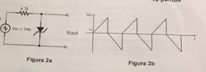
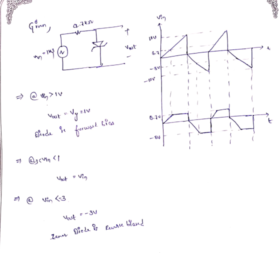
For the circuit of figure 2a, draw the waveform on the diode (Vout) for the input voltage of figure 2b. Assume a forward breakdown voltage Vy = 1V and a Zener voltage Vz = 3V.
Homework Answers
Add Answer to:
For the circuit of figure 2a, draw the waveform on the diode
(Vout) for the input...
4. Design a clamp circuit to clamp the negative extreme of a periodic input waveform of 10 sin(100πt)V to −5 V. Use 1 diode, 1 Zener diode, 1 resistor, and 1 capacitor of suitable values. Provide foll...
4. Design a clamp circuit to clamp the negative extreme of a periodic input waveform of 10 sin(100πt)V to −5 V. Use 1 diode, 1 Zener diode, 1 resistor, and 1 capacitor of suitable values. Provide following minimum ratings of the selected components. (a) Diode - Maximum reverse voltage, peak forward current (b) Zener - Zener voltage, Zener current (c) Resistor - Resistance, power rating (d) capacitor - capacitance, Maximum voltage Assume a 0.6 V forward drop for all diodes...
For the double diode circuit shown in figure 2-1, answer the following questions. In Figure 2-1...
 For the double diode circuit shown in figure 2-1, answer the following questions. In Figure 2-1 a) (10pts) For the triangular wave input shown (Vin), sketch the output voltage (Vout) using the constant voltage drop model (CVD: Vo-0.7V). Be sure to note the voltage values on the y-axis of your Vout plot and show any equations you used to determine those values ime FEE 334: Spring 2019 Midterm b) (2pts) During the middle of the first time segment (when Vin...
All used in the next circuit diodes are silicon. Zener of diode D2 the voltage is...
 All used in the next circuit diodes are silicon. Zener of diode
D2 the voltage is 8 V, the zener voltage of the D4 diode is 5.6 V
It is given as. Applied input voltage Vin = 20 sin (ωt) is
determined as V. Output of the circuit voltage changes according to
the applied voltage of Vin Analyze the circuit and draw it.
(Simplified of diode element model will be used.) (I can't analyze.
Please explain)
R + D D3...
All used in the next circuit diodes are silicon. Zener of diode
D2 the voltage is 8 V, the zener voltage of the D4 diode is 5.6 V
It is given as. Applied input voltage Vin = 20 sin (ωt) is
determined as V. Output of the circuit voltage changes according to
the applied voltage of Vin Analyze the circuit and draw it.
(Simplified of diode element model will be used.) (I can't analyze.
Please explain)
R + D D3...
a) Use the constant voltage drop model for the diode and determine the input / output...
 a) Use the constant voltage drop model for the diode and
determine the input / output ratio (Vout x Vin), equations. Vdon =
0.7V, rz = 0Ω, Vz = 3V and R = R1 = R2 = 1000Ω.
b) Draw the Vout x Vin graph. Highlight the slope coefficients
of the lines and the coordinates of the points where the slope
changes occur.
D1 D2 DR3 Vin 7R1 Vout 214 22
a) Use the constant voltage drop model for the diode and
determine the input / output ratio (Vout x Vin), equations. Vdon =
0.7V, rz = 0Ω, Vz = 3V and R = R1 = R2 = 1000Ω.
b) Draw the Vout x Vin graph. Highlight the slope coefficients
of the lines and the coordinates of the points where the slope
changes occur.
D1 D2 DR3 Vin 7R1 Vout 214 22
Draw in detail the waveform at the output (Vo) of the circuit in Figure 2. Then...
 Draw in detail the waveform at the output (Vo) of the circuit in
Figure 2. Then obtain the maximum current flowing through the Zener
diode. Consider that all diodes (including the Zener) behave like
direct bias Silicon diodes. For reverse bias the Zener voltage is
8.6 V; all other diodes never conduct in reverse bias. The input
voltage is a 1 Hz triangular signal with values from -20V to
20V.
1k Vo 1Hz
Draw in detail the waveform at the output (Vo) of the circuit in
Figure 2. Then obtain the maximum current flowing through the Zener
diode. Consider that all diodes (including the Zener) behave like
direct bias Silicon diodes. For reverse bias the Zener voltage is
8.6 V; all other diodes never conduct in reverse bias. The input
voltage is a 1 Hz triangular signal with values from -20V to
20V.
1k Vo 1Hz
Please answer clearly Determine voltage characteristics (Vout/V) of the circuit shown in Figure 1. Assume: a)...
 Please answer clearly
Determine voltage characteristics (Vout/V) of the circuit shown in Figure 1. Assume: a) Diodes D1 and D2 are ideal. b) Zener diode has r2-0 with the break down voltage of Vz-12 V. 1ΚΩ D1 D2 추 R2 1ΚΩ Vout Figure 1
Please answer clearly
Determine voltage characteristics (Vout/V) of the circuit shown in Figure 1. Assume: a) Diodes D1 and D2 are ideal. b) Zener diode has r2-0 with the break down voltage of Vz-12 V. 1ΚΩ D1 D2 추 R2 1ΚΩ Vout Figure 1
Ctri Question 3 (20 Marks) Lab 1-Zener Circuits and Applications Theory: Zener diode is designed ...
 Ctri Question 3 (20 Marks) Lab 1-Zener Circuits and Applications Theory: Zener diode is designed to operate in reverse conduction. Zener breakdown occurs at a precisely defined voltage, allowing the diode to be used as a voltage reference or clipper. While Zener diodes are usually operated in reverse conduction, they may also be operated in cutoff and forward conduction. There are two different effects that are used in "Zener diodes". The only practical difference is that the two types have...
1. For the 4 circuits shown below, sketch the output waveform for a 1V peak, 1kHz,...
 1. For the 4 circuits shown below, sketch the output waveform for a 1V peak, 1kHz, sinusoidal wave in put signal. Assume the diodes are ideal and they exhibit ON-OFF switch model behaviour. Create an ideal diode model in LT-Spice with the following specification [.model IdealDiode D(Ron=0.1m Roff=100G Vfwd-0.0) ] simulate the circuit and verify the output waveform. Vin Vout Vin Vout 1k 1k (a) (b) 1k Vin 1k Vin Vout Vout ww 1k (c) (d) KH
1. For the...
1. For the 4 circuits shown below, sketch the output waveform for a 1V peak, 1kHz, sinusoidal wave in put signal. Assume the diodes are ideal and they exhibit ON-OFF switch model behaviour. Create an ideal diode model in LT-Spice with the following specification [.model IdealDiode D(Ron=0.1m Roff=100G Vfwd-0.0) ] simulate the circuit and verify the output waveform. Vin Vout Vin Vout 1k 1k (a) (b) 1k Vin 1k Vin Vout Vout ww 1k (c) (d) KH
1. For the...
breakdown, with respect to the input voltag. 4. BONUS: Fig. 5 presents a half sinusoidal, with...
 breakdown, with respect to the input voltag. 4. BONUS: Fig. 5 presents a half sinusoidal, with 2V peak-to-peak, no DC offset. Fig. 5 presents a half wave rectifier. We assume Vin here is aw the Vout waveform when the diode has 0.7V voltage drop. Diode + 7 + vin Load Svout AC Voltage vir Source Fig.5. Half wave rectifier circuit
Design a diode waveform shaping circuit that would have the above transfer function. You can use...
 Design a diode waveform shaping circuit that would have the
above transfer function. You can use PN junction diodes with VD0 =
0.7 V, DC voltage sources, and resistors in your design. You should
indicate the resistor values and the DC voltage sources’ values in
your design if you used any resistors or DC voltage sources. You
can use Zener diodes with different Vz values if you want, but you
do not have to.
Write the possible cases of the...
Design a diode waveform shaping circuit that would have the
above transfer function. You can use PN junction diodes with VD0 =
0.7 V, DC voltage sources, and resistors in your design. You should
indicate the resistor values and the DC voltage sources’ values in
your design if you used any resistors or DC voltage sources. You
can use Zener diodes with different Vz values if you want, but you
do not have to.
Write the possible cases of the...
 For the double diode circuit shown in figure 2-1, answer the following questions. In Figure 2-1 a) (10pts) For the triangular wave input shown (Vin), sketch the output voltage (Vout) using the constant voltage drop model (CVD: Vo-0.7V). Be sure to note the voltage values on the y-axis of your Vout plot and show any equations you used to determine those values ime FEE 334: Spring 2019 Midterm b) (2pts) During the middle of the first time segment (when Vin...
 All used in the next circuit diodes are silicon. Zener of diode
D2 the voltage is 8 V, the zener voltage of the D4 diode is 5.6 V
It is given as. Applied input voltage Vin = 20 sin (ωt) is
determined as V. Output of the circuit voltage changes according to
the applied voltage of Vin Analyze the circuit and draw it.
(Simplified of diode element model will be used.) (I can't analyze.
Please explain)
R + D D3...
All used in the next circuit diodes are silicon. Zener of diode
D2 the voltage is 8 V, the zener voltage of the D4 diode is 5.6 V
It is given as. Applied input voltage Vin = 20 sin (ωt) is
determined as V. Output of the circuit voltage changes according to
the applied voltage of Vin Analyze the circuit and draw it.
(Simplified of diode element model will be used.) (I can't analyze.
Please explain)
R + D D3...
 a) Use the constant voltage drop model for the diode and
determine the input / output ratio (Vout x Vin), equations. Vdon =
0.7V, rz = 0Ω, Vz = 3V and R = R1 = R2 = 1000Ω.
b) Draw the Vout x Vin graph. Highlight the slope coefficients
of the lines and the coordinates of the points where the slope
changes occur.
D1 D2 DR3 Vin 7R1 Vout 214 22
a) Use the constant voltage drop model for the diode and
determine the input / output ratio (Vout x Vin), equations. Vdon =
0.7V, rz = 0Ω, Vz = 3V and R = R1 = R2 = 1000Ω.
b) Draw the Vout x Vin graph. Highlight the slope coefficients
of the lines and the coordinates of the points where the slope
changes occur.
D1 D2 DR3 Vin 7R1 Vout 214 22
 Draw in detail the waveform at the output (Vo) of the circuit in
Figure 2. Then obtain the maximum current flowing through the Zener
diode. Consider that all diodes (including the Zener) behave like
direct bias Silicon diodes. For reverse bias the Zener voltage is
8.6 V; all other diodes never conduct in reverse bias. The input
voltage is a 1 Hz triangular signal with values from -20V to
20V.
1k Vo 1Hz
Draw in detail the waveform at the output (Vo) of the circuit in
Figure 2. Then obtain the maximum current flowing through the Zener
diode. Consider that all diodes (including the Zener) behave like
direct bias Silicon diodes. For reverse bias the Zener voltage is
8.6 V; all other diodes never conduct in reverse bias. The input
voltage is a 1 Hz triangular signal with values from -20V to
20V.
1k Vo 1Hz
 Please answer clearly
Determine voltage characteristics (Vout/V) of the circuit shown in Figure 1. Assume: a) Diodes D1 and D2 are ideal. b) Zener diode has r2-0 with the break down voltage of Vz-12 V. 1ΚΩ D1 D2 추 R2 1ΚΩ Vout Figure 1
Please answer clearly
Determine voltage characteristics (Vout/V) of the circuit shown in Figure 1. Assume: a) Diodes D1 and D2 are ideal. b) Zener diode has r2-0 with the break down voltage of Vz-12 V. 1ΚΩ D1 D2 추 R2 1ΚΩ Vout Figure 1
 Ctri Question 3 (20 Marks) Lab 1-Zener Circuits and Applications Theory: Zener diode is designed to operate in reverse conduction. Zener breakdown occurs at a precisely defined voltage, allowing the diode to be used as a voltage reference or clipper. While Zener diodes are usually operated in reverse conduction, they may also be operated in cutoff and forward conduction. There are two different effects that are used in "Zener diodes". The only practical difference is that the two types have...
 1. For the 4 circuits shown below, sketch the output waveform for a 1V peak, 1kHz, sinusoidal wave in put signal. Assume the diodes are ideal and they exhibit ON-OFF switch model behaviour. Create an ideal diode model in LT-Spice with the following specification [.model IdealDiode D(Ron=0.1m Roff=100G Vfwd-0.0) ] simulate the circuit and verify the output waveform. Vin Vout Vin Vout 1k 1k (a) (b) 1k Vin 1k Vin Vout Vout ww 1k (c) (d) KH
1. For the...
1. For the 4 circuits shown below, sketch the output waveform for a 1V peak, 1kHz, sinusoidal wave in put signal. Assume the diodes are ideal and they exhibit ON-OFF switch model behaviour. Create an ideal diode model in LT-Spice with the following specification [.model IdealDiode D(Ron=0.1m Roff=100G Vfwd-0.0) ] simulate the circuit and verify the output waveform. Vin Vout Vin Vout 1k 1k (a) (b) 1k Vin 1k Vin Vout Vout ww 1k (c) (d) KH
1. For the...
 breakdown, with respect to the input voltag. 4. BONUS: Fig. 5 presents a half sinusoidal, with 2V peak-to-peak, no DC offset. Fig. 5 presents a half wave rectifier. We assume Vin here is aw the Vout waveform when the diode has 0.7V voltage drop. Diode + 7 + vin Load Svout AC Voltage vir Source Fig.5. Half wave rectifier circuit
 Design a diode waveform shaping circuit that would have the
above transfer function. You can use PN junction diodes with VD0 =
0.7 V, DC voltage sources, and resistors in your design. You should
indicate the resistor values and the DC voltage sources’ values in
your design if you used any resistors or DC voltage sources. You
can use Zener diodes with different Vz values if you want, but you
do not have to.
Write the possible cases of the...
Design a diode waveform shaping circuit that would have the
above transfer function. You can use PN junction diodes with VD0 =
0.7 V, DC voltage sources, and resistors in your design. You should
indicate the resistor values and the DC voltage sources’ values in
your design if you used any resistors or DC voltage sources. You
can use Zener diodes with different Vz values if you want, but you
do not have to.
Write the possible cases of the...
Most questions answered within 3 hours.
-
The University of
Texas recently reported that 43% of college students aged 18-24
would spend their...
asked 56 minutes ago -
The length of stay at a specific emergency department in
Phoenix, Arizona, in 2009 had a...
asked 12 minutes ago -
. Please give the mechanism for this type of problem. Step by
Step
The toxin that...
asked 15 minutes ago -
If you have a 1M stock solution and you want to dilute 1 :10
with water,...
asked 17 minutes ago -
In a load instruction, the effective address is obtained by
A) Retriving the address from a...
asked 17 minutes ago -
Use the following information to answer this question.
Windswept, Inc. 2017 Income Statement ($ in millions)...
asked 18 minutes ago -
A mutual fund salesperson has arranged to call on four people
tomorrow. Based on past experience...
asked 52 minutes ago -
Let the RV Y has the pdf
f ( y ) = 6 y ( 1...
asked 1 hour ago -
Question 12
Where should a copy of a private key should be placed so it is...
asked 20 minutes ago -
What is the entropy change to the surroundings when 1 mol of ice
melts in someone's...
asked 40 minutes ago -
Pt1
An electrochemical cell is set up at 25°C based on the overall
reaction represented by...
asked 46 minutes ago -
Explain traveling wave theory. Explain how the peaking of the
wave leads to action potentials and...
asked 37 minutes ago