
Homework Answers
Solution:
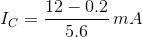
Given that

Given:


- Base-Emitter Junction is forward biased.
- Therefore, transistor operate either in saturation (or) in active region.
- Assume, it is in active region.


KVL: 


 Collector junction is forward biased.
Transistor is in saturation region.

KVL : 

KVL:- 
Add Answer to:
2. (20 points) In the circuit shown below the silicon transistor has B=70. (a) Determine Ib,...
3. For the circuit shown a. Determine the levels of IB, Ic and Vce for the...
 3. For the circuit shown a. Determine the levels of IB, Ic and Vce for the circuit shown. b. Change B to 150 (36.4% increase), and calculate the new levels of IB, Ic and VCE. c. Determine the magnitude of the percentage change in Ic and VCE +24 V 470 k 2 B = 110
Problem 4 (20 %) For the circuit shown in Figure 4 determine IB, IC, and VC....
 Problem 4 (20 %) For the circuit shown in Figure 4 determine IB,
IC, and VC. Data VCC=9 V VBB=4 V R2= 165 k R1= 2.5 k Transistor
Assume VBE ≈ 0.7 V and =150
Derive all the results. Give the answers with the preestablished
prefix.
FAVOR DIBUJAR LOS CIRCUITOS
Problem 4 (206) For the circuit shown in Figure 4 determine IB, I, and Vc. Data Ve=9 V V=4V R = 165 kg R=2.5k_2 Transistor Assume VE 0.7 V and...
Problem 4 (20 %) For the circuit shown in Figure 4 determine IB,
IC, and VC. Data VCC=9 V VBB=4 V R2= 165 k R1= 2.5 k Transistor
Assume VBE ≈ 0.7 V and =150
Derive all the results. Give the answers with the preestablished
prefix.
FAVOR DIBUJAR LOS CIRCUITOS
Problem 4 (206) For the circuit shown in Figure 4 determine IB, I, and Vc. Data Ve=9 V V=4V R = 165 kg R=2.5k_2 Transistor Assume VE 0.7 V and...
Problem: In the circuit shown in Figure 1, Vee = 1.2 V, Vcc = 20 V,...
 Problem: In the circuit shown in Figure 1, Vee = 1.2 V, Vcc = 20 V, Rp = 60 kN, Rc = 2 k. The input signal is a sinusoidal voltage given by Vin(t) = 0.2 sin(2000 ) V. The input and output characteristics of the transistor are provided on Page 2. (1) Find Ig, Ic and Vce. (30 points) Hint: Use the load line method. (Vor.) and (Vce: 1c) are the operating points of the transistor in the input...
The component values for the npn-transistor amplifier circuit are R = 665 Q, Vcc= 20 V,...
 The component values for the npn-transistor amplifier circuit are R = 665 Q, Vcc= 20 V, VB= 2.4 V, and RB= 85k a) The graphon the last page shows the characteristics for the transistor in the above circuit Construct the load line for th is transistor circuit and draw it into the IC vs. VCE graph. Briefly state how you determine the load line. b) Determine the base current, assuming that the transistor is made of silicon. c) Determine the...
Problem 4a (15 points) For the transistor circuit shown in the figure, calculate the value of...
 Problem 4a (15 points) For the transistor circuit shown in the figure, calculate the value of the output voltage given β 49 and VBE-0.7V. Problem 4b (10 points) The charge entering an electric element (part) is shown in the figure. Find the current at t- 1.5 sec, t-2.5 sec and t 10 sec 30 0 246810 12 Problem 3 (25 points) For the circuit shown in the Figure, use the Mesh Analysis method, to find the value of the branch...
1) Calculate the value of the base current IB. (in μA) 2) Calculate the value of...
 1) Calculate the value of the base current
IB. (in μA)
2) Calculate the value of the base collector current
IC. (In mA)
3) Calculate the value of the collector-emitter voltage
VCE. (In V)
Required information In the circuit below: RB = 820 kN, Vcc = 12 V, RC = 3 kN2, and Bdc = 100. Note: The transistor is silicon. Vcc w Rc Re Bdc
1) Calculate the value of the base current
IB. (in μA)
2) Calculate the value of the base collector current
IC. (In mA)
3) Calculate the value of the collector-emitter voltage
VCE. (In V)
Required information In the circuit below: RB = 820 kN, Vcc = 12 V, RC = 3 kN2, and Bdc = 100. Note: The transistor is silicon. Vcc w Rc Re Bdc
np transistor with an α of 0.9925 is based in the circuit shown below with a...
 np transistor with an α of 0.9925 is based in the circuit shown below with a (12 points) 3, A p base current of 40μΑ. Determine β, Ic, and IE. Ic V CE
(13 points) For the transistor in the circuit shown below, VBE(on) = 0.7 V, Vce(sat) =...
 (13 points) For the transistor in the circuit shown below, VBE(on) = 0.7 V, Vce(sat) = 0.2 V, and B = 100. Determine the value of the collector current. +5 V R=1.2 ko R =33 k2 -5 V
Experiment 2: Good biasing Set up the circuit with R2 12 k2, R RE 1 k, and Vcc 15 V 39 k2, Rc = 2 k?. Circuit An...
 Experiment 2: Good biasing Set up the circuit with R2 12 k2, R RE 1 k, and Vcc 15 V 39 k2, Rc = 2 k?. Circuit Analysis: Compute Ic, I, and VCE PSpice Simulation: a) Simulate the circuit with PSpice (bias point details only) and compare values of Ic, IB, VCE, and VBE from PSpice simulations with your analytical calculations. b) Rerun your PSpice simulations for temperatures of 0 and 60°C. Make a table of Ic IB, VCE, and...
D. For the transistor circuit shown in Figure 7, assuming that the transistor is in the...
 D. For the transistor circuit shown in Figure 7, assuming that the transistor is in the forward active mode, and B = 100 and VBE = 0.7V, calculate Base current 1B Collector current Ic (iii) Emitter current le (iv) Collector to emitter voltage Vce and (v) Voltage across the 2009 resistor v 3 80022 10 kV W VCE VBE مت + + 1 2001} 1 1
 3. For the circuit shown a. Determine the levels of IB, Ic and Vce for the circuit shown. b. Change B to 150 (36.4% increase), and calculate the new levels of IB, Ic and VCE. c. Determine the magnitude of the percentage change in Ic and VCE +24 V 470 k 2 B = 110
 Problem 4 (20 %) For the circuit shown in Figure 4 determine IB,
IC, and VC. Data VCC=9 V VBB=4 V R2= 165 k R1= 2.5 k Transistor
Assume VBE ≈ 0.7 V and =150
Derive all the results. Give the answers with the preestablished
prefix.
FAVOR DIBUJAR LOS CIRCUITOS
Problem 4 (206) For the circuit shown in Figure 4 determine IB, I, and Vc. Data Ve=9 V V=4V R = 165 kg R=2.5k_2 Transistor Assume VE 0.7 V and...
Problem 4 (20 %) For the circuit shown in Figure 4 determine IB,
IC, and VC. Data VCC=9 V VBB=4 V R2= 165 k R1= 2.5 k Transistor
Assume VBE ≈ 0.7 V and =150
Derive all the results. Give the answers with the preestablished
prefix.
FAVOR DIBUJAR LOS CIRCUITOS
Problem 4 (206) For the circuit shown in Figure 4 determine IB, I, and Vc. Data Ve=9 V V=4V R = 165 kg R=2.5k_2 Transistor Assume VE 0.7 V and...
 Problem: In the circuit shown in Figure 1, Vee = 1.2 V, Vcc = 20 V, Rp = 60 kN, Rc = 2 k. The input signal is a sinusoidal voltage given by Vin(t) = 0.2 sin(2000 ) V. The input and output characteristics of the transistor are provided on Page 2. (1) Find Ig, Ic and Vce. (30 points) Hint: Use the load line method. (Vor.) and (Vce: 1c) are the operating points of the transistor in the input...
 The component values for the npn-transistor amplifier circuit are R = 665 Q, Vcc= 20 V, VB= 2.4 V, and RB= 85k a) The graphon the last page shows the characteristics for the transistor in the above circuit Construct the load line for th is transistor circuit and draw it into the IC vs. VCE graph. Briefly state how you determine the load line. b) Determine the base current, assuming that the transistor is made of silicon. c) Determine the...
 Problem 4a (15 points) For the transistor circuit shown in the figure, calculate the value of the output voltage given β 49 and VBE-0.7V. Problem 4b (10 points) The charge entering an electric element (part) is shown in the figure. Find the current at t- 1.5 sec, t-2.5 sec and t 10 sec 30 0 246810 12 Problem 3 (25 points) For the circuit shown in the Figure, use the Mesh Analysis method, to find the value of the branch...
 1) Calculate the value of the base current
IB. (in μA)
2) Calculate the value of the base collector current
IC. (In mA)
3) Calculate the value of the collector-emitter voltage
VCE. (In V)
Required information In the circuit below: RB = 820 kN, Vcc = 12 V, RC = 3 kN2, and Bdc = 100. Note: The transistor is silicon. Vcc w Rc Re Bdc
1) Calculate the value of the base current
IB. (in μA)
2) Calculate the value of the base collector current
IC. (In mA)
3) Calculate the value of the collector-emitter voltage
VCE. (In V)
Required information In the circuit below: RB = 820 kN, Vcc = 12 V, RC = 3 kN2, and Bdc = 100. Note: The transistor is silicon. Vcc w Rc Re Bdc
 np transistor with an α of 0.9925 is based in the circuit shown below with a (12 points) 3, A p base current of 40μΑ. Determine β, Ic, and IE. Ic V CE
 (13 points) For the transistor in the circuit shown below, VBE(on) = 0.7 V, Vce(sat) = 0.2 V, and B = 100. Determine the value of the collector current. +5 V R=1.2 ko R =33 k2 -5 V
 Experiment 2: Good biasing Set up the circuit with R2 12 k2, R RE 1 k, and Vcc 15 V 39 k2, Rc = 2 k?. Circuit Analysis: Compute Ic, I, and VCE PSpice Simulation: a) Simulate the circuit with PSpice (bias point details only) and compare values of Ic, IB, VCE, and VBE from PSpice simulations with your analytical calculations. b) Rerun your PSpice simulations for temperatures of 0 and 60°C. Make a table of Ic IB, VCE, and...
 D. For the transistor circuit shown in Figure 7, assuming that the transistor is in the forward active mode, and B = 100 and VBE = 0.7V, calculate Base current 1B Collector current Ic (iii) Emitter current le (iv) Collector to emitter voltage Vce and (v) Voltage across the 2009 resistor v 3 80022 10 kV W VCE VBE مت + + 1 2001} 1 1
Most questions answered within 3 hours.
-
Do elephants and cows present an interesting dichotomy when
viewed from the perspective of property rights?
asked 1 minute ago -
USE an API
You have a drop down list of 4 cities.
Upon selecting a particular...
asked 1 minute ago -
Which type of chemical reaction is regulated by altering an
enzyme's function?
a.) irreversible
b.) reversible
asked 4 minutes ago -
Supply management is a developing ____________ and an area of
management _______________.
1. discipline / responsibility...
asked 7 minutes ago -
Calculate the mass of acetic acid that must be mixed with
0.88moles of sodium acetate to...
asked 8 minutes ago -
Crown Corporation, a United States Company, made a sale to a
foreign customer on
September 15,...
asked 9 minutes ago -
The complete combustion of acetic acid, HC2H3O2(l) to form
H2O(l) and CO2(g) at constant pressure releases...
asked 21 minutes ago -
What is the effect of using MACRS rather than straight-line
depreciation?
It increases the NPV.
The...
asked 19 minutes ago -
Write a program to create a game map. A game map is a 2D array
of...
asked 29 minutes ago -
2. When a student ran an asymmetric dihydroxylation reaction
using cis-stilbene and the ligand (DHQ)2PHAL, the...
asked 28 minutes ago -
The daily closing price of FPT stock over last year would
be:
A.Time series data
B.Cross...
asked 43 minutes ago -
A hair is placed at one edge between two flat glass plates 10.7
cm long. When...
asked 42 minutes ago