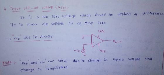
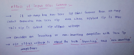
what is the meaning and cause of input offset voltage and bias current. different compensation methods
Homework Answers


Add Answer to:
what is the meaning and cause of input offset voltage and bias
current. different compensation methods
c) In estimating DC imperfections (input offset voltage, input offset current and the inverting amplifier with...
 c) In estimating DC imperfections (input offset voltage, input offset current and the inverting amplifier with nominal gain of -100 using 1 current) of an op-map, an and 10MQ resistors is implemented using the op-amp as shown in Fig 2(a) below R2 10MQ R 100k Vi Vo Figure 2(a): Inverting amplifier Measurements are conducted on the output voltage of the inverting amplifier under the following conditions: (i) the input (V) is open circuited and the output voltage is found to...
Please choose the correct responses below: The input offset voltage is proportional to temperature changes and the mismatch in load resistors An active load circuit is a current mirror with improved...
 Please choose the correct responses below: The input offset voltage is proportional to temperature changes and the mismatch in load resistors An active load circuit is a current mirror with improved voltage gain for single ended output, stability via negative feedback and saves area on an IC The differential output CMRR of a matched MOSFET pair depends on the output impedance of current source providing bias at the common source. Input offset bias current is caused by mismatch in temperature...
3-13. For the circuit of Problem 3-9 (Figure P3-9), assume that the op-amp bias and offset para m...
 3-13 please
3-13. For the circuit of Problem 3-9 (Figure P3-9), assume that the op-amp bias and offset para meters are as follows: Input offset voltage 1.2 mV Input bias current-60 nA Input offset current 8 nA a. Determine the magnitude of the output de voltage al produced, by the input offiset b. With Rc 0, determine the magnitude of the output de voltage al produced by the inp (You may now assume the ideal gain equation from Chapter 2...
3-13 please
3-13. For the circuit of Problem 3-9 (Figure P3-9), assume that the op-amp bias and offset para meters are as follows: Input offset voltage 1.2 mV Input bias current-60 nA Input offset current 8 nA a. Determine the magnitude of the output de voltage al produced, by the input offiset b. With Rc 0, determine the magnitude of the output de voltage al produced by the inp (You may now assume the ideal gain equation from Chapter 2...
What are the Input impedance, output impedance, voltage gain and current gain equations for a common...
What are the Input impedance, output impedance, voltage gain and current gain equations for a common emitter amplifier biased using emitter bias? (Plus please provide the circuit)
a) Determine the DC bias voltage Vce and the current Ic for the voltage divider configuration...
 a) Determine the DC bias voltage Vce and the current Ic for the voltage divider configuration in Fig. 11. [4.0 marks] +22 V 10 k92 39k92 10 F HE 10 uF ti VE B = 100 3.9 k2 50uF Figure 11 b) Provide the construction diagram of n-channel JFET ii. n-channel depletion type MOSFET iii. n-channel Enhancement type MOSFET i. [3.0 marks) c) Describe the operation of an NPN transistor in the common-emitter (CE) configuration with aid of input and...
a) Using the constant voltage drop (CVD) model, what is the minimum input voltage that can...
 a) Using the constant voltage
drop (CVD) model, what is the minimum input
voltage that can reach the MOS circuitry before a diode
turns on, shunting the current to ground? (At this point you
can assume R1 = R2 = 0Ω)
b) Using the constant voltage drop (CVD) model, what is the
maximum input voltage that can reach the MOS
circuitry before a diode turns on, shunting the current to the
supply (Vdd)? (At this point you can assume R1...
a) Using the constant voltage
drop (CVD) model, what is the minimum input
voltage that can reach the MOS circuitry before a diode
turns on, shunting the current to ground? (At this point you
can assume R1 = R2 = 0Ω)
b) Using the constant voltage drop (CVD) model, what is the
maximum input voltage that can reach the MOS
circuitry before a diode turns on, shunting the current to the
supply (Vdd)? (At this point you can assume R1...
2. For the circuit shown below, find the current ip and voltage V1. Assume the forward bias volta...
 2. For the circuit shown below, find the current ip and voltage V1. Assume the forward bias voltage of the diode is 0.7V V1 5 V 5 V
2. For the circuit shown below, find the current ip and voltage V1. Assume the forward bias voltage of the diode is 0.7V V1 5 V 5 V
2. For the circuit shown below, find the current ip and voltage V1. Assume the forward bias voltage of the diode is 0.7V V1 5 V 5 V
Denve faih exmession VI + GIven the llowis Op Auf. en SKetch and abel axis tue...
 Denve faih exmession VI + GIven the llowis Op Auf. en SKetch and abel axis tue Picture" G Bu rAPh db 2.1 Model Parameters for the LM741 and the OPA300 Opamp amp Model "LM741" Library "LM 2 x 10⁵ 2 x 10⁶ Open-loop gain Input resistance Output resistance Positive voltage swing Negative voltage swing Input offset voltage Input bias current 75 21 -21 V 50 V 0.001 8 x 10⁻⁸ A 2x 10⁻⁸ 5 x 10⁵ 1.5 x 10⁶ 4.5x...
Problem 3: a) For the inverting amplifier designed using low noise amplifier AD743 shown on the...
Problem 3: a) For the inverting amplifier designed using low noise amplifier AD743 shown on the bottom of the page with Ri=10kOhm and Rf=220kOhm, what should be the value of the resistor connected to the non-inverting input (R2) to minimize the output offset due to input bias current? b.) Even if the R2 value you calculated is used, could there be an output offset due to a difference between the two input bias currents? What is the maximum value of...
1a. What current flow (I) is associated with an input voltage of 5.0V and resistors R1...
1a. What current flow (I) is associated with an input voltage of 5.0V and resistors R1 = 1.5 kiloohms and R2 = 0.5 kiloohms? Calculate this value in mA. 1b. What current flow (I) is associated with an input voltage of 8.0V and resistors R1 = 2.5 kiloohms and R2 = 3.5 kiloohms? Calculate this value in mA 1c. What is the voltage across R2 with an input voltage of 5.0V and resistors R1 = 1.5 kiloohms and R2 =...
 c) In estimating DC imperfections (input offset voltage, input offset current and the inverting amplifier with nominal gain of -100 using 1 current) of an op-map, an and 10MQ resistors is implemented using the op-amp as shown in Fig 2(a) below R2 10MQ R 100k Vi Vo Figure 2(a): Inverting amplifier Measurements are conducted on the output voltage of the inverting amplifier under the following conditions: (i) the input (V) is open circuited and the output voltage is found to...
 Please choose the correct responses below: The input offset voltage is proportional to temperature changes and the mismatch in load resistors An active load circuit is a current mirror with improved voltage gain for single ended output, stability via negative feedback and saves area on an IC The differential output CMRR of a matched MOSFET pair depends on the output impedance of current source providing bias at the common source. Input offset bias current is caused by mismatch in temperature...
 3-13 please
3-13. For the circuit of Problem 3-9 (Figure P3-9), assume that the op-amp bias and offset para meters are as follows: Input offset voltage 1.2 mV Input bias current-60 nA Input offset current 8 nA a. Determine the magnitude of the output de voltage al produced, by the input offiset b. With Rc 0, determine the magnitude of the output de voltage al produced by the inp (You may now assume the ideal gain equation from Chapter 2...
3-13 please
3-13. For the circuit of Problem 3-9 (Figure P3-9), assume that the op-amp bias and offset para meters are as follows: Input offset voltage 1.2 mV Input bias current-60 nA Input offset current 8 nA a. Determine the magnitude of the output de voltage al produced, by the input offiset b. With Rc 0, determine the magnitude of the output de voltage al produced by the inp (You may now assume the ideal gain equation from Chapter 2...
 a) Determine the DC bias voltage Vce and the current Ic for the voltage divider configuration in Fig. 11. [4.0 marks] +22 V 10 k92 39k92 10 F HE 10 uF ti VE B = 100 3.9 k2 50uF Figure 11 b) Provide the construction diagram of n-channel JFET ii. n-channel depletion type MOSFET iii. n-channel Enhancement type MOSFET i. [3.0 marks) c) Describe the operation of an NPN transistor in the common-emitter (CE) configuration with aid of input and...
 a) Using the constant voltage
drop (CVD) model, what is the minimum input
voltage that can reach the MOS circuitry before a diode
turns on, shunting the current to ground? (At this point you
can assume R1 = R2 = 0Ω)
b) Using the constant voltage drop (CVD) model, what is the
maximum input voltage that can reach the MOS
circuitry before a diode turns on, shunting the current to the
supply (Vdd)? (At this point you can assume R1...
a) Using the constant voltage
drop (CVD) model, what is the minimum input
voltage that can reach the MOS circuitry before a diode
turns on, shunting the current to ground? (At this point you
can assume R1 = R2 = 0Ω)
b) Using the constant voltage drop (CVD) model, what is the
maximum input voltage that can reach the MOS
circuitry before a diode turns on, shunting the current to the
supply (Vdd)? (At this point you can assume R1...
 2. For the circuit shown below, find the current ip and voltage V1. Assume the forward bias voltage of the diode is 0.7V V1 5 V 5 V
2. For the circuit shown below, find the current ip and voltage V1. Assume the forward bias voltage of the diode is 0.7V V1 5 V 5 V
2. For the circuit shown below, find the current ip and voltage V1. Assume the forward bias voltage of the diode is 0.7V V1 5 V 5 V
 Denve faih exmession VI + GIven the llowis Op Auf. en SKetch and abel axis tue Picture" G Bu rAPh db 2.1 Model Parameters for the LM741 and the OPA300 Opamp amp Model "LM741" Library "LM 2 x 10⁵ 2 x 10⁶ Open-loop gain Input resistance Output resistance Positive voltage swing Negative voltage swing Input offset voltage Input bias current 75 21 -21 V 50 V 0.001 8 x 10⁻⁸ A 2x 10⁻⁸ 5 x 10⁵ 1.5 x 10⁶ 4.5x...
Most questions answered within 3 hours.
-
Garcia Company issues 20.00%, 15-year bonds with a par value of
$470,000 and semiannual interest payments....
asked 6 minutes ago -
The price of 1 lb of potatoes is $1.75. If all the potatoes sold
today at...
asked 8 minutes ago -
In C++ Programming, Try using loops only.
This lab demonstrates the use of the While Loop...
asked 55 minutes ago -
Effect of DCMU and sodium azide on Chlamydomonas? We did an
experiment where we had Chlamydomonas...
asked 1 hour ago -
1a) According to the ideal gas law, _______________.
a. a gas has infinite volume at absolute...
asked 3 hours ago -
Oakdale Fashions, Inc. had $245,000 in 2018 taxable income.
Using the tax schedule in Table 2.3...
asked 3 hours ago -
The marketing class at CSUS had an average score of 150. An
educational analyst determined that...
asked 4 hours ago -
Justin Case has purchased a $250 000 home by putting 20 % down
and taking out...
asked 4 hours ago -
1. In a labor market, marginal cost for a firm is
____________.
a. recruiting cost
b....
asked 5 hours ago -
On January 1, 2019, ABC Company issued $60,000,000 of 20-year,
10.5% bonds when the market rate...
asked 5 hours ago -
39.4% of US homes continue to use a landline in addition to cell
phone service. 3...
asked 6 hours ago -
Starting with benzene, synthesize 1-phenyl-1-butyne.
Show intermediates and reagents.
asked 7 hours ago