![[P.4] Calculate all node voltage and branch current and small-signal parameters with voltage gain for each of the circuits de](http://img.homeworklib.com/questions/4a1ecdd0-eee6-11eb-82bb-7d619c5005fc.png?x-oss-process=image/resize,w_560)
Homework Answers


Add Answer to:
[P.4] Calculate all node voltage and branch current and small-signal parameters with voltage gain for each...
Calculate the voltage gain (Av) for the loaded Common Emitter Amplifier below: BAC 200 for all...
 Calculate the voltage gain (Av) for the loaded Common Emitter Amplifier below: BAC 200 for all transistors. Assume re 15 Q for the CE Amplifier. Ignore re' for the DP Amplifier Vcc 12 V, R1 56 K, R2 10 KQ, R4 22 KQ R3 5.6 KQ, RL 8 RE(CE) 628 0, RE(CC) 330 Rc 3.5 KQ, Enter your results. No units. SR3 R1 RC C3 Vcc C1 Beta Q2a HH Vin Beta Q1 Beta Q2b C4 R4 Vs R2 C2...
The circu with (WL)1-4 50/0.5 and Iss 21 0.5 mA. (a) Calculate the small-signal voltage gain. (b)...
 The circu with (WL)1-4 50/0.5 and Iss 21 0.5 mA. (a) Calculate the small-signal voltage gain. (b) Determine the maximum output voltage swing if the input CM level is 1.3 V. Figure 5.23 (a) Differential pair with current-source load; (b) circuit for calculation of Gmi (c) circuit for calculation of Rout uit of Fig. 5.23(a) is designed VDD M3 M4 Vout Vin Iss
The circu with (WL)1-4 50/0.5 and Iss 21 0.5 mA. (a) Calculate the small-signal voltage gain. (b)...
The circu with (WL)1-4 50/0.5 and Iss 21 0.5 mA. (a) Calculate the small-signal voltage gain. (b) Determine the maximum output voltage swing if the input CM level is 1.3 V. Figure 5.23 (a) Differential pair with current-source load; (b) circuit for calculation of Gmi (c) circuit for calculation of Rout uit of Fig. 5.23(a) is designed VDD M3 M4 Vout Vin Iss
The circu with (WL)1-4 50/0.5 and Iss 21 0.5 mA. (a) Calculate the small-signal voltage gain. (b)...
1-Clear handwriting 2-Correct answer 3-Organized 4-answer all the questions Please Problem 2 On the circuit on...
 1-Clear handwriting
2-Correct answer
3-Organized
4-answer all the questions
Please
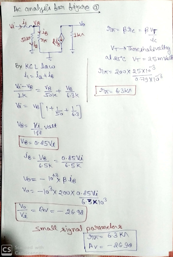
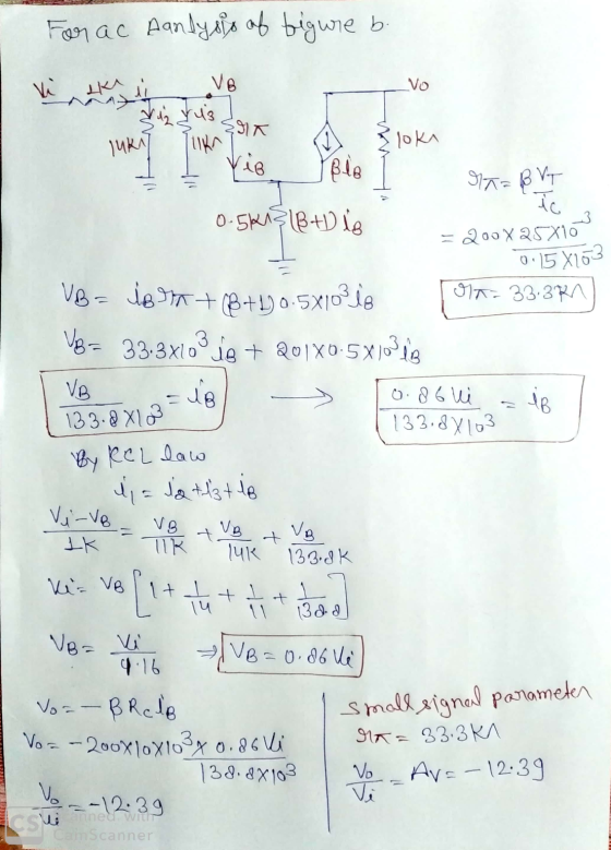
Problem 2 On the circuit on Figure P2, transi stor Q1 has a threshold voltage of Vt = 2 V and a transconductance parameter of k = 100 mA/V2. Note that Vcc = -Vee = 4.5 V. Moreover, capacitors C1, C2, and C3 can be assumed to be very large VDD 4.5.0 R3 25kQ R1 300kn C2 Vout C1 Rsig Q1 1k0 R2 200kn Vsig (R4 2kQ C3 -4.5V VSS...
1-Clear handwriting
2-Correct answer
3-Organized
4-answer all the questions
Please
Problem 2 On the circuit on Figure P2, transi stor Q1 has a threshold voltage of Vt = 2 V and a transconductance parameter of k = 100 mA/V2. Note that Vcc = -Vee = 4.5 V. Moreover, capacitors C1, C2, and C3 can be assumed to be very large VDD 4.5.0 R3 25kQ R1 300kn C2 Vout C1 Rsig Q1 1k0 R2 200kn Vsig (R4 2kQ C3 -4.5V VSS...
Voc Ri Rc C2 + RS G Q2N3904 RL Vout 2 R2 RE CE Rin Rout...
 Voc Ri Rc C2 + RS G Q2N3904 RL Vout 2 R2 RE CE Rin Rout Cu B 1x B C o + V be : Cr 8m'be E VCC R R2 Rc RE RS RL С. Cz CE 12 V 8.2 kg 3.9 ko 6.3 k2 3.3 kΩ 3 ko 3.9 ko 10 uF 1uF 100 u Assume the 2N3904 has a 8 =100, Veron} = 0.7V, VA= 100V, C=100, C=13.9pF and Ce=8pF. Use the emission coefficient as n...
Homework 4 Due: June 26, 2019, at 5 pm. Note: Show all steps required to get...
 Homework 4 Due: June 26, 2019, at 5 pm. Note: Show all steps required to get to your answers and make sure to box them. Writing down answers to questions asked without any explanation(s) will not do it. Clarity should be a priority Moreover, the assigned textbook for this class is Sedra and Smith, Microelectronic Circuits, Seventh Edition, Oxford University Press. Make sure you have the proper book Reminder: In class, we have expressed the overall voltage gain of a...
Homework 4 Due: June 26, 2019, at 5 pm. Note: Show all steps required to get...
 Homework 4 Due: June 26, 2019, at 5 pm. Note: Show all steps required to get to your answers and make sure to box them. Writing down answers to questions asked without any explanation(s) will not do it. Clarity should be a priority Moreover, the assigned textbook for this class is Sedra and Smith, Microelectronic Circuits, Seventh Edition, Oxford Univers ity Press. Make sure you have the proper book Reminder: In class, we have expressed the overall voltage gain of...
 Calculate the voltage gain (Av) for the loaded Common Emitter Amplifier below: BAC 200 for all transistors. Assume re 15 Q for the CE Amplifier. Ignore re' for the DP Amplifier Vcc 12 V, R1 56 K, R2 10 KQ, R4 22 KQ R3 5.6 KQ, RL 8 RE(CE) 628 0, RE(CC) 330 Rc 3.5 KQ, Enter your results. No units. SR3 R1 RC C3 Vcc C1 Beta Q2a HH Vin Beta Q1 Beta Q2b C4 R4 Vs R2 C2...
 The circu with (WL)1-4 50/0.5 and Iss 21 0.5 mA. (a) Calculate the small-signal voltage gain. (b) Determine the maximum output voltage swing if the input CM level is 1.3 V. Figure 5.23 (a) Differential pair with current-source load; (b) circuit for calculation of Gmi (c) circuit for calculation of Rout uit of Fig. 5.23(a) is designed VDD M3 M4 Vout Vin Iss
The circu with (WL)1-4 50/0.5 and Iss 21 0.5 mA. (a) Calculate the small-signal voltage gain. (b)...
The circu with (WL)1-4 50/0.5 and Iss 21 0.5 mA. (a) Calculate the small-signal voltage gain. (b) Determine the maximum output voltage swing if the input CM level is 1.3 V. Figure 5.23 (a) Differential pair with current-source load; (b) circuit for calculation of Gmi (c) circuit for calculation of Rout uit of Fig. 5.23(a) is designed VDD M3 M4 Vout Vin Iss
The circu with (WL)1-4 50/0.5 and Iss 21 0.5 mA. (a) Calculate the small-signal voltage gain. (b)...
 1-Clear handwriting
2-Correct answer
3-Organized
4-answer all the questions
Please
Problem 2 On the circuit on Figure P2, transi stor Q1 has a threshold voltage of Vt = 2 V and a transconductance parameter of k = 100 mA/V2. Note that Vcc = -Vee = 4.5 V. Moreover, capacitors C1, C2, and C3 can be assumed to be very large VDD 4.5.0 R3 25kQ R1 300kn C2 Vout C1 Rsig Q1 1k0 R2 200kn Vsig (R4 2kQ C3 -4.5V VSS...
1-Clear handwriting
2-Correct answer
3-Organized
4-answer all the questions
Please
Problem 2 On the circuit on Figure P2, transi stor Q1 has a threshold voltage of Vt = 2 V and a transconductance parameter of k = 100 mA/V2. Note that Vcc = -Vee = 4.5 V. Moreover, capacitors C1, C2, and C3 can be assumed to be very large VDD 4.5.0 R3 25kQ R1 300kn C2 Vout C1 Rsig Q1 1k0 R2 200kn Vsig (R4 2kQ C3 -4.5V VSS...
 Voc Ri Rc C2 + RS G Q2N3904 RL Vout 2 R2 RE CE Rin Rout Cu B 1x B C o + V be : Cr 8m'be E VCC R R2 Rc RE RS RL С. Cz CE 12 V 8.2 kg 3.9 ko 6.3 k2 3.3 kΩ 3 ko 3.9 ko 10 uF 1uF 100 u Assume the 2N3904 has a 8 =100, Veron} = 0.7V, VA= 100V, C=100, C=13.9pF and Ce=8pF. Use the emission coefficient as n...
 Homework 4 Due: June 26, 2019, at 5 pm. Note: Show all steps required to get to your answers and make sure to box them. Writing down answers to questions asked without any explanation(s) will not do it. Clarity should be a priority Moreover, the assigned textbook for this class is Sedra and Smith, Microelectronic Circuits, Seventh Edition, Oxford University Press. Make sure you have the proper book Reminder: In class, we have expressed the overall voltage gain of a...
 Homework 4 Due: June 26, 2019, at 5 pm. Note: Show all steps required to get to your answers and make sure to box them. Writing down answers to questions asked without any explanation(s) will not do it. Clarity should be a priority Moreover, the assigned textbook for this class is Sedra and Smith, Microelectronic Circuits, Seventh Edition, Oxford Univers ity Press. Make sure you have the proper book Reminder: In class, we have expressed the overall voltage gain of...
Most questions answered within 3 hours.
-
Calculate the number density of argon gas at a temperature of
24C and a pressure of...
asked 1 hour ago -
Alternative
Classification
How to Estimate
Probabilities from Data? ( For continuous Attributes)
And How to generate...
asked 2 hours ago -
An explosion breaks a 20.0-kg object into three parts. The
object is initially moving at a...
asked 2 hours ago -
Calculate the approximate number of residues of Rubisco, which
is involved in carbon fixation in plants,...
asked 3 hours ago -
Other decisions about scientific claims can have a much broader
impact.ENERGYarrow-10x10.png, environment, health, security - all...
asked 4 hours ago -
I need to write a research paper and work cited about this
topic: The United States...
asked 5 hours ago -
Hello! I was wondering if I could have some help?
If the vapor pressure of carvone...
asked 5 hours ago -
An economist wants to estimate the mean per capita income (in
thousands of dollars) for a...
asked 5 hours ago -
What would be the input/output characteristic of a circuit
obtained by putting two of your 2's-complementers...
asked 5 hours ago -
In Drosophila, the transition from the syncytial blastoderm
stage to the cellular blastoderm stage is a...
asked 6 hours ago -
Project management question:
Name 3 different types of resources (hint: humans are one
type)
asked 6 hours ago -
Consider the following reaction: C 2H 2( g) + 2H 2( g) C 2H 6(
g)...
asked 6 hours ago