1-Clear handwriting
2-Correct answer
3-Organized
4-answer all the questions
Please
Homework Answers

Add Answer to:
1-Clear handwriting
2-Correct answer
3-Organized
4-answer all the questions
Please
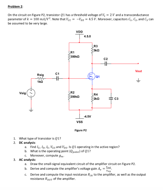
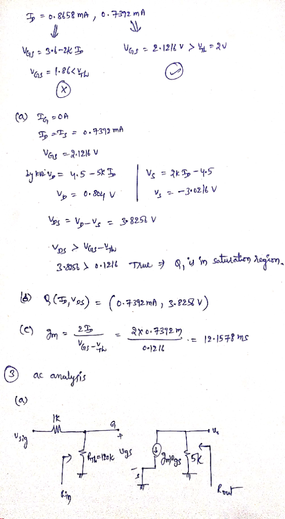
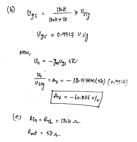
Problem 2 On the circuit on...
Problem 3: 1. 2. What kind of amplifier (given what you have studied in class) is the circuit on ...
 Problem 3: 1. 2. What kind of amplifier (given what you have studied in class) is the circuit on Figure P3? Why? Draw the small-signal equivalent circuit of the amplifier circuit on Figure P3 operating at mid- band frequencies. V1 C2 V2 Vout Q2 R3 R1 C1 Rsig Q1 Vsig R2 Figure P3
Problem 3: 1. 2. What kind of amplifier (given what you have studied in class) is the circuit on Figure P3? Why? Draw the small-signal equivalent circuit...
Problem 3: 1. 2. What kind of amplifier (given what you have studied in class) is the circuit on Figure P3? Why? Draw the small-signal equivalent circuit of the amplifier circuit on Figure P3 operating at mid- band frequencies. V1 C2 V2 Vout Q2 R3 R1 C1 Rsig Q1 Vsig R2 Figure P3
Problem 3: 1. 2. What kind of amplifier (given what you have studied in class) is the circuit on Figure P3? Why? Draw the small-signal equivalent circuit...
Problem 2 Consider the feedback amplifier circuit on Figure P2. The DC current gain of transistor Q3 is -100 1. What type of feedback (or what feedback topology) do we have on the circuit in Figure P...
 Problem 2 Consider the feedback amplifier circuit on Figure P2. The DC current gain of transistor Q3 is -100 1. What type of feedback (or what feedback topology) do we have on the circuit in Figure P2? 2. Draw the A-circuit. Express and compute the open-loop voltage gain A at mid-band frequency 3, Draw the γ-circuit. Express and compute the feedback factor γ 4. Express and compute the overall gain of the feedback amplifier Ap Express and compute the input...
Score 2. (22 points) For the circuit in Figure 2, the transistor parameters are: 2 0,...
 Score 2. (22 points) For the circuit in Figure 2, the transistor parameters are: 2 0, VN=2V, Ka-1mA/V2, all the capacitors are assumed to act as short circuits at the signal frequency (1) Calculate the Q-point (Vos. I Vos); (2) Sketch the small-signal equivalent circuit, you must label the polarities of the voltages and the direction of the current; (3) Determine the voltage gain A, vo/v (4) Determine the input resistance Ri and output resistance Ro V1 5 10 V...
Problem 2: Consider the following amplifier circuit. All capacitors are infinite valued. Voc RB1 Rc1 Rc2...
 Problem 2: Consider the following amplifier circuit. All capacitors are infinite valued. Voc RB1 Rc1 Rc2 0 Q1 Vout RB2 Rout1 Q2 Rout2 Rint R1 Rin2 Rsig + IEI Vsig Voc SINE() IE2 a. Specify the type of amplifier in each stage. b. Draw the small signal model of this amplifier and include the early effect. c. Derive an expression for Rout1 and Rout2 including early effect. d. Derive expressions for Rin1 and Rin2. Ignore the early effect. e. Derive...
Problem 2: In the circuit on Figure P2, BJT NPN Q1 and Q2 emulate a Darlington...
 Problem 2: In the circuit on Figure P2, BJT NPN Q1 and Q2 emulate a Darlington Pair (DP). It should be noted that Q1 and Q2 are such that their current gains are B1 B2 = B = 99. Moreover, capacitors C1 and C2 can be assumed to be very large. Note: The DC analysis of the DP circuit below can be done in a similar fashion as what you do when only dealing with one transistor. Express the current...
Note Show all steps required to get to your answers and make sure to box them....
 Note Show all steps required to get to your answers and make sure to box them. Writing down answers to questions asked without any explanation(s) will not do it. Clarity should be a priority Moreover, the assigned textbook for this class is Sedra and Smith, Microelectronic Circuits, Seventh Edition, Oxford University Press. Make sure you have the proper book Problem 3: What kind of amplifier (given what you have studied in class) is the circuit on Figure P3? Why? 1....
Homework 4 Due: June 26, 2019, at 5 pm. Note: Show all steps required to get...
 Homework 4 Due: June 26, 2019, at 5 pm. Note: Show all steps required to get to your answers and make sure to box them. Writing down answers to questions asked without any explanation(s) will not do it. Clarity should be a priority Moreover, the assigned textbook for this class is Sedra and Smith, Microelectronic Circuits, Seventh Edition, Oxford University Press. Make sure you have the proper book Reminder: In class, we have expressed the overall voltage gain of a...
1-Clear handwriting 2-Correct answer 3-Organized 4-answer all the questions Please Note Show all steps required to...
 1-Clear handwriting
2-Correct answer
3-Organized
4-answer all the questions
Please
Note Show all steps required to get to your answers and make sure to box them. Writing down answers to questions asked without any explanation(s) will not do it. Clarity should be a priority When/If drawing, fully annotate your drawing, as you will be graded on the clarity of the drawing Moreover, the assigned textbook for this class is Sedra and Smith, Microelectronic Circuits, Seventh Edition, Oxford University Press. Make...
1-Clear handwriting
2-Correct answer
3-Organized
4-answer all the questions
Please
Note Show all steps required to get to your answers and make sure to box them. Writing down answers to questions asked without any explanation(s) will not do it. Clarity should be a priority When/If drawing, fully annotate your drawing, as you will be graded on the clarity of the drawing Moreover, the assigned textbook for this class is Sedra and Smith, Microelectronic Circuits, Seventh Edition, Oxford University Press. Make...
Problem 3: Design Problem On Figure P3a, you have a Common Source (CS) n-channel MOSFET amplifier....
 Problem 3: Design Problem On Figure P3a, you have a Common Source (CS) n-channel MOSFET amplifier. Notice the absence of a source resistor Rsig and load resistor R. If we know how the present amplifier (the one on Figure P3a) behaves without Rsig and RL, we can infer its behaviors if Rsig and R were to be added. design the amplifier circuit on Figure P3a, i.e., you have to find appropriate values for RGj You are to RG,, RD, and...
Homework 4 Due: June 26, 2019, at 5 pm. Note: Show all steps required to get...
 Homework 4 Due: June 26, 2019, at 5 pm. Note: Show all steps required to get to your answers and make sure to box them. Writing down answers to questions asked without any explanation(s) will not do it. Clarity should be a priority Moreover, the assigned textbook for this class is Sedra and Smith, Microelectronic Circuits, Seventh Edition, Oxford Univers ity Press. Make sure you have the proper book Reminder: In class, we have expressed the overall voltage gain of...
 Problem 3: 1. 2. What kind of amplifier (given what you have studied in class) is the circuit on Figure P3? Why? Draw the small-signal equivalent circuit of the amplifier circuit on Figure P3 operating at mid- band frequencies. V1 C2 V2 Vout Q2 R3 R1 C1 Rsig Q1 Vsig R2 Figure P3
Problem 3: 1. 2. What kind of amplifier (given what you have studied in class) is the circuit on Figure P3? Why? Draw the small-signal equivalent circuit...
Problem 3: 1. 2. What kind of amplifier (given what you have studied in class) is the circuit on Figure P3? Why? Draw the small-signal equivalent circuit of the amplifier circuit on Figure P3 operating at mid- band frequencies. V1 C2 V2 Vout Q2 R3 R1 C1 Rsig Q1 Vsig R2 Figure P3
Problem 3: 1. 2. What kind of amplifier (given what you have studied in class) is the circuit on Figure P3? Why? Draw the small-signal equivalent circuit...
 Problem 2 Consider the feedback amplifier circuit on Figure P2. The DC current gain of transistor Q3 is -100 1. What type of feedback (or what feedback topology) do we have on the circuit in Figure P2? 2. Draw the A-circuit. Express and compute the open-loop voltage gain A at mid-band frequency 3, Draw the γ-circuit. Express and compute the feedback factor γ 4. Express and compute the overall gain of the feedback amplifier Ap Express and compute the input...
 Score 2. (22 points) For the circuit in Figure 2, the transistor parameters are: 2 0, VN=2V, Ka-1mA/V2, all the capacitors are assumed to act as short circuits at the signal frequency (1) Calculate the Q-point (Vos. I Vos); (2) Sketch the small-signal equivalent circuit, you must label the polarities of the voltages and the direction of the current; (3) Determine the voltage gain A, vo/v (4) Determine the input resistance Ri and output resistance Ro V1 5 10 V...
 Problem 2: Consider the following amplifier circuit. All capacitors are infinite valued. Voc RB1 Rc1 Rc2 0 Q1 Vout RB2 Rout1 Q2 Rout2 Rint R1 Rin2 Rsig + IEI Vsig Voc SINE() IE2 a. Specify the type of amplifier in each stage. b. Draw the small signal model of this amplifier and include the early effect. c. Derive an expression for Rout1 and Rout2 including early effect. d. Derive expressions for Rin1 and Rin2. Ignore the early effect. e. Derive...
 Problem 2: In the circuit on Figure P2, BJT NPN Q1 and Q2 emulate a Darlington Pair (DP). It should be noted that Q1 and Q2 are such that their current gains are B1 B2 = B = 99. Moreover, capacitors C1 and C2 can be assumed to be very large. Note: The DC analysis of the DP circuit below can be done in a similar fashion as what you do when only dealing with one transistor. Express the current...
 Note Show all steps required to get to your answers and make sure to box them. Writing down answers to questions asked without any explanation(s) will not do it. Clarity should be a priority Moreover, the assigned textbook for this class is Sedra and Smith, Microelectronic Circuits, Seventh Edition, Oxford University Press. Make sure you have the proper book Problem 3: What kind of amplifier (given what you have studied in class) is the circuit on Figure P3? Why? 1....
 Homework 4 Due: June 26, 2019, at 5 pm. Note: Show all steps required to get to your answers and make sure to box them. Writing down answers to questions asked without any explanation(s) will not do it. Clarity should be a priority Moreover, the assigned textbook for this class is Sedra and Smith, Microelectronic Circuits, Seventh Edition, Oxford University Press. Make sure you have the proper book Reminder: In class, we have expressed the overall voltage gain of a...
 1-Clear handwriting
2-Correct answer
3-Organized
4-answer all the questions
Please
Note Show all steps required to get to your answers and make sure to box them. Writing down answers to questions asked without any explanation(s) will not do it. Clarity should be a priority When/If drawing, fully annotate your drawing, as you will be graded on the clarity of the drawing Moreover, the assigned textbook for this class is Sedra and Smith, Microelectronic Circuits, Seventh Edition, Oxford University Press. Make...
1-Clear handwriting
2-Correct answer
3-Organized
4-answer all the questions
Please
Note Show all steps required to get to your answers and make sure to box them. Writing down answers to questions asked without any explanation(s) will not do it. Clarity should be a priority When/If drawing, fully annotate your drawing, as you will be graded on the clarity of the drawing Moreover, the assigned textbook for this class is Sedra and Smith, Microelectronic Circuits, Seventh Edition, Oxford University Press. Make...
 Problem 3: Design Problem On Figure P3a, you have a Common Source (CS) n-channel MOSFET amplifier. Notice the absence of a source resistor Rsig and load resistor R. If we know how the present amplifier (the one on Figure P3a) behaves without Rsig and RL, we can infer its behaviors if Rsig and R were to be added. design the amplifier circuit on Figure P3a, i.e., you have to find appropriate values for RGj You are to RG,, RD, and...
 Homework 4 Due: June 26, 2019, at 5 pm. Note: Show all steps required to get to your answers and make sure to box them. Writing down answers to questions asked without any explanation(s) will not do it. Clarity should be a priority Moreover, the assigned textbook for this class is Sedra and Smith, Microelectronic Circuits, Seventh Edition, Oxford Univers ity Press. Make sure you have the proper book Reminder: In class, we have expressed the overall voltage gain of...
Most questions answered within 3 hours.
-
The length of stay at a specific emergency department in
Phoenix, Arizona, in 2009 had a...
asked 59 seconds ago -
. Please give the mechanism for this type of problem. Step by
Step
The toxin that...
asked 4 minutes ago -
If you have a 1M stock solution and you want to dilute 1 :10
with water,...
asked 6 minutes ago -
In a load instruction, the effective address is obtained by
A) Retriving the address from a...
asked 6 minutes ago -
Use the following information to answer this question.
Windswept, Inc. 2017 Income Statement ($ in millions)...
asked 7 minutes ago -
A mutual fund salesperson has arranged to call on four people
tomorrow. Based on past experience...
asked 40 minutes ago -
Let the RV Y has the pdf
f ( y ) = 6 y ( 1...
asked 52 minutes ago -
Question 12
Where should a copy of a private key should be placed so it is...
asked 9 minutes ago -
What is the entropy change to the surroundings when 1 mol of ice
melts in someone's...
asked 28 minutes ago -
Pt1
An electrochemical cell is set up at 25°C based on the overall
reaction represented by...
asked 35 minutes ago -
Explain traveling wave theory. Explain how the peaking of the
wave leads to action potentials and...
asked 26 minutes ago -
If you mixed 35.0 mLmL of 0.100 M Tris-HCl with 65.0
mLmL of 0.200 M Tris-base, what would...
asked 22 minutes ago