

Homework Answers
Add Answer to:
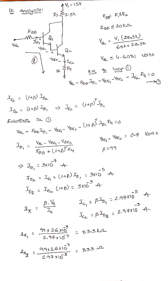
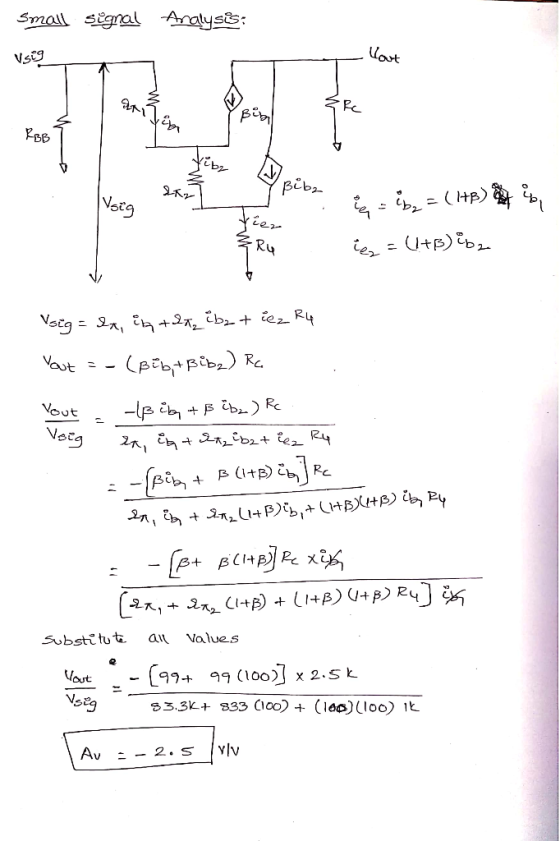
Problem 2: In the circuit on Figure P2, BJT NPN Q1 and Q2 emulate a Darlington...
Question I : Consider the amplifier circuit shown below (p-150 for both transistors) (18 marks) +12V R4 1k8 R1 15k Q1 2N3904 C2+ 10μ R2 6V 4k7 2mA Out Q2 2N3904 C1 R3 10k R5 1k8 In 10H (i) Perform...
 Question I : Consider the amplifier circuit shown below (p-150 for both transistors) (18 marks) +12V R4 1k8 R1 15k Q1 2N3904 C2+ 10μ R2 6V 4k7 2mA Out Q2 2N3904 C1 R3 10k R5 1k8 In 10H (i) Perform DC analysis and prove that the indicated voltages and currents in the figure are correctly calculated. Find the operating point of Q1 and Q2 (5 marks) (ii) Calculate the gain of this amplifier (5 marks) (iii) In the lab, only...
Consider the BJT circuit below with Qi and Q2 being identical transistors with Bac oc 50....
 Consider the BJT circuit below with Qi and Q2 being identical transistors with Bac oc 50. Assume a Vcc of 10 volts. 10 kS2 21 R6 C. 22 k? 4.7 k? a) Do a DC analysis on the Qi circuit and solve all B, C and E terminal voltages and currents. Use the quick analysis method after checking if the loading of R4 and R6 is acceptable b) Do a DC analysis on the Q2 circuit and solve all B,...
Consider the BJT circuit below with Qi and Q2 being identical transistors with Bac oc 50....
 Consider the BJT circuit below with Qi and Q2 being identical transistors with Bac oc 50. Assume a Vcc of 10 volts. 10 kS2 21 R6 C. 22 kΩ 4.7 kΩ a) Do a DC analysis on the Qi circuit and solve all B, C and E terminal voltages and currents. Use the quick analysis method after checking if the loading of R4 and R6 is acceptable b) Do a DC analysis on the Q2 circuit and solve all B,...
4. Consider the Darlington circuit shown. 12V R1 4.3ΜΩ C1 Bo-9000 QVBED-1.4V Q2 C2 4302 a) Find the DC values of Ici, Ic2, Vcei, VcE2, P1, and P2. b) Determine the input impedance, output impedance,...
 4. Consider the Darlington circuit shown. 12V R1 4.3ΜΩ C1 Bo-9000 QVBED-1.4V Q2 C2 4302 a) Find the DC values of Ici, Ic2, Vcei, VcE2, P1, and P2. b) Determine the input impedance, output impedance, and no-load voltage gain for this circuit.
4. Consider the Darlington circuit shown. 12V R1 4.3ΜΩ C1 Bo-9000 QVBED-1.4V Q2 C2 4302 a) Find the DC values of Ici, Ic2, Vcei, VcE2, P1, and P2. b) Determine the input impedance, output impedance, and no-load voltage...
4. Consider the Darlington circuit shown. 12V R1 4.3ΜΩ C1 Bo-9000 QVBED-1.4V Q2 C2 4302 a) Find the DC values of Ici, Ic2, Vcei, VcE2, P1, and P2. b) Determine the input impedance, output impedance, and no-load voltage gain for this circuit.
4. Consider the Darlington circuit shown. 12V R1 4.3ΜΩ C1 Bo-9000 QVBED-1.4V Q2 C2 4302 a) Find the DC values of Ici, Ic2, Vcei, VcE2, P1, and P2. b) Determine the input impedance, output impedance, and no-load voltage...
1-Clear handwriting 2-Correct answer 3-Organized 4-answer all the questions Please Problem 2 On the circuit on...
 1-Clear handwriting
2-Correct answer
3-Organized
4-answer all the questions
Please
Problem 2 On the circuit on Figure P2, transi stor Q1 has a threshold voltage of Vt = 2 V and a transconductance parameter of k = 100 mA/V2. Note that Vcc = -Vee = 4.5 V. Moreover, capacitors C1, C2, and C3 can be assumed to be very large VDD 4.5.0 R3 25kQ R1 300kn C2 Vout C1 Rsig Q1 1k0 R2 200kn Vsig (R4 2kQ C3 -4.5V VSS...
1-Clear handwriting
2-Correct answer
3-Organized
4-answer all the questions
Please
Problem 2 On the circuit on Figure P2, transi stor Q1 has a threshold voltage of Vt = 2 V and a transconductance parameter of k = 100 mA/V2. Note that Vcc = -Vee = 4.5 V. Moreover, capacitors C1, C2, and C3 can be assumed to be very large VDD 4.5.0 R3 25kQ R1 300kn C2 Vout C1 Rsig Q1 1k0 R2 200kn Vsig (R4 2kQ C3 -4.5V VSS...
2. For the follower circuit below, KNOWN AS A Darlington pair, let Vcc 9V VBEON0.6V, and B100, VA for both transist...
 2. For the follower circuit below, KNOWN AS A Darlington pair, let Vcc 9V VBEON0.6V, and B100, VA for both transistors. a. Find each transistor operating point. b. If a load resistor of R 1ks2 is connected to the output terminal (RL not shown in the figure), find the voltage gain from the base of Q2 to the output, and the input resistance looking into the base of Q2 (R2). Hint: Consider Q2 as an emitter follower fed by a...
Problem 3: 1. 2. What kind of amplifier (given what you have studied in class) is the circuit on ...
 Problem 3: 1. 2. What kind of amplifier (given what you have studied in class) is the circuit on Figure P3? Why? Draw the small-signal equivalent circuit of the amplifier circuit on Figure P3 operating at mid- band frequencies. V1 C2 V2 Vout Q2 R3 R1 C1 Rsig Q1 Vsig R2 Figure P3
Problem 3: 1. 2. What kind of amplifier (given what you have studied in class) is the circuit on Figure P3? Why? Draw the small-signal equivalent circuit...
Problem 3: 1. 2. What kind of amplifier (given what you have studied in class) is the circuit on Figure P3? Why? Draw the small-signal equivalent circuit of the amplifier circuit on Figure P3 operating at mid- band frequencies. V1 C2 V2 Vout Q2 R3 R1 C1 Rsig Q1 Vsig R2 Figure P3
Problem 3: 1. 2. What kind of amplifier (given what you have studied in class) is the circuit on Figure P3? Why? Draw the small-signal equivalent circuit...
Consider the electric circuit shown in the figure. Assume that the voltage of the battery is...
 Consider the electric circuit shown in the figure. Assume that
the voltage of the battery is V = 23.5 V, and the resistors are
R1 = R2 = R3 = R4 =
R5 = 2.00 Ω.
What is the equivalent resistance of the circuit?
What is the electric current flowing through resistor
R3?
Consider the electri = R4 = R5 = 2.00 2 circuit shown in the figure. Assume that the voltage of the battery is V = 23.5 V,...
Consider the electric circuit shown in the figure. Assume that
the voltage of the battery is V = 23.5 V, and the resistors are
R1 = R2 = R3 = R4 =
R5 = 2.00 Ω.
What is the equivalent resistance of the circuit?
What is the electric current flowing through resistor
R3?
Consider the electri = R4 = R5 = 2.00 2 circuit shown in the figure. Assume that the voltage of the battery is V = 23.5 V,...
Problem 2 Consider the feedback amplifier circuit on Figure P2. The DC current gain of transistor Q3 is -100 1. What type of feedback (or what feedback topology) do we have on the circuit in Figure P...
 Problem 2 Consider the feedback amplifier circuit on Figure P2. The DC current gain of transistor Q3 is -100 1. What type of feedback (or what feedback topology) do we have on the circuit in Figure P2? 2. Draw the A-circuit. Express and compute the open-loop voltage gain A at mid-band frequency 3, Draw the γ-circuit. Express and compute the feedback factor γ 4. Express and compute the overall gain of the feedback amplifier Ap Express and compute the input...
 Question I : Consider the amplifier circuit shown below (p-150 for both transistors) (18 marks) +12V R4 1k8 R1 15k Q1 2N3904 C2+ 10μ R2 6V 4k7 2mA Out Q2 2N3904 C1 R3 10k R5 1k8 In 10H (i) Perform DC analysis and prove that the indicated voltages and currents in the figure are correctly calculated. Find the operating point of Q1 and Q2 (5 marks) (ii) Calculate the gain of this amplifier (5 marks) (iii) In the lab, only...
 Consider the BJT circuit below with Qi and Q2 being identical transistors with Bac oc 50. Assume a Vcc of 10 volts. 10 kS2 21 R6 C. 22 k? 4.7 k? a) Do a DC analysis on the Qi circuit and solve all B, C and E terminal voltages and currents. Use the quick analysis method after checking if the loading of R4 and R6 is acceptable b) Do a DC analysis on the Q2 circuit and solve all B,...
 Consider the BJT circuit below with Qi and Q2 being identical transistors with Bac oc 50. Assume a Vcc of 10 volts. 10 kS2 21 R6 C. 22 kΩ 4.7 kΩ a) Do a DC analysis on the Qi circuit and solve all B, C and E terminal voltages and currents. Use the quick analysis method after checking if the loading of R4 and R6 is acceptable b) Do a DC analysis on the Q2 circuit and solve all B,...
 4. Consider the Darlington circuit shown. 12V R1 4.3ΜΩ C1 Bo-9000 QVBED-1.4V Q2 C2 4302 a) Find the DC values of Ici, Ic2, Vcei, VcE2, P1, and P2. b) Determine the input impedance, output impedance, and no-load voltage gain for this circuit.
4. Consider the Darlington circuit shown. 12V R1 4.3ΜΩ C1 Bo-9000 QVBED-1.4V Q2 C2 4302 a) Find the DC values of Ici, Ic2, Vcei, VcE2, P1, and P2. b) Determine the input impedance, output impedance, and no-load voltage...
4. Consider the Darlington circuit shown. 12V R1 4.3ΜΩ C1 Bo-9000 QVBED-1.4V Q2 C2 4302 a) Find the DC values of Ici, Ic2, Vcei, VcE2, P1, and P2. b) Determine the input impedance, output impedance, and no-load voltage gain for this circuit.
4. Consider the Darlington circuit shown. 12V R1 4.3ΜΩ C1 Bo-9000 QVBED-1.4V Q2 C2 4302 a) Find the DC values of Ici, Ic2, Vcei, VcE2, P1, and P2. b) Determine the input impedance, output impedance, and no-load voltage...
 1-Clear handwriting
2-Correct answer
3-Organized
4-answer all the questions
Please
Problem 2 On the circuit on Figure P2, transi stor Q1 has a threshold voltage of Vt = 2 V and a transconductance parameter of k = 100 mA/V2. Note that Vcc = -Vee = 4.5 V. Moreover, capacitors C1, C2, and C3 can be assumed to be very large VDD 4.5.0 R3 25kQ R1 300kn C2 Vout C1 Rsig Q1 1k0 R2 200kn Vsig (R4 2kQ C3 -4.5V VSS...
1-Clear handwriting
2-Correct answer
3-Organized
4-answer all the questions
Please
Problem 2 On the circuit on Figure P2, transi stor Q1 has a threshold voltage of Vt = 2 V and a transconductance parameter of k = 100 mA/V2. Note that Vcc = -Vee = 4.5 V. Moreover, capacitors C1, C2, and C3 can be assumed to be very large VDD 4.5.0 R3 25kQ R1 300kn C2 Vout C1 Rsig Q1 1k0 R2 200kn Vsig (R4 2kQ C3 -4.5V VSS...
 2. For the follower circuit below, KNOWN AS A Darlington pair, let Vcc 9V VBEON0.6V, and B100, VA for both transistors. a. Find each transistor operating point. b. If a load resistor of R 1ks2 is connected to the output terminal (RL not shown in the figure), find the voltage gain from the base of Q2 to the output, and the input resistance looking into the base of Q2 (R2). Hint: Consider Q2 as an emitter follower fed by a...
 Problem 3: 1. 2. What kind of amplifier (given what you have studied in class) is the circuit on Figure P3? Why? Draw the small-signal equivalent circuit of the amplifier circuit on Figure P3 operating at mid- band frequencies. V1 C2 V2 Vout Q2 R3 R1 C1 Rsig Q1 Vsig R2 Figure P3
Problem 3: 1. 2. What kind of amplifier (given what you have studied in class) is the circuit on Figure P3? Why? Draw the small-signal equivalent circuit...
Problem 3: 1. 2. What kind of amplifier (given what you have studied in class) is the circuit on Figure P3? Why? Draw the small-signal equivalent circuit of the amplifier circuit on Figure P3 operating at mid- band frequencies. V1 C2 V2 Vout Q2 R3 R1 C1 Rsig Q1 Vsig R2 Figure P3
Problem 3: 1. 2. What kind of amplifier (given what you have studied in class) is the circuit on Figure P3? Why? Draw the small-signal equivalent circuit...
 Consider the electric circuit shown in the figure. Assume that
the voltage of the battery is V = 23.5 V, and the resistors are
R1 = R2 = R3 = R4 =
R5 = 2.00 Ω.
What is the equivalent resistance of the circuit?
What is the electric current flowing through resistor
R3?
Consider the electri = R4 = R5 = 2.00 2 circuit shown in the figure. Assume that the voltage of the battery is V = 23.5 V,...
Consider the electric circuit shown in the figure. Assume that
the voltage of the battery is V = 23.5 V, and the resistors are
R1 = R2 = R3 = R4 =
R5 = 2.00 Ω.
What is the equivalent resistance of the circuit?
What is the electric current flowing through resistor
R3?
Consider the electri = R4 = R5 = 2.00 2 circuit shown in the figure. Assume that the voltage of the battery is V = 23.5 V,...
 Problem 2 Consider the feedback amplifier circuit on Figure P2. The DC current gain of transistor Q3 is -100 1. What type of feedback (or what feedback topology) do we have on the circuit in Figure P2? 2. Draw the A-circuit. Express and compute the open-loop voltage gain A at mid-band frequency 3, Draw the γ-circuit. Express and compute the feedback factor γ 4. Express and compute the overall gain of the feedback amplifier Ap Express and compute the input...
Most questions answered within 3 hours.
-
(Expected rate of return and risk) Carter Inc. is evaluating a
security. Calculate the investment’s expected...
asked 2 hours ago -
What specific indicators can point to lack of progress for
African Americans in American society?
asked 3 hours ago -
1-The Electrons in a beam are moving at 2.7×10⁸ m/s in an
electric field of 15000...
asked 3 hours ago -
A gas tank is a vertical cylinder. It has a radius of 1m, a
height of...
asked 3 hours ago -
Accent Software faces the following conditions. All of these
support Accent’s use of a market-penetration pricing...
asked 4 hours ago -
A mathematically inclined friend emails you the following
instructions: "Meet me in the cafeteria the first...
asked 4 hours ago -
A monopoly sells in two countries . The demand curves in the two
countries are p1...
asked 5 hours ago -
A .15kg rubber ball is bounced off a wall. Before hitting the
wall, the ball moves...
asked 6 hours ago -
A manufacturing company preparing to build a new plant is
considering three potential locations for it....
asked 6 hours ago -
B. If compound Y has approximately the same values of solubility
in toluene as compound X,...
asked 7 hours ago -
Oscar Inc. has inventory in Japan valued at 39,051,000 Yen one
year ago. One year ago...
asked 7 hours ago -
If Canada suffered from "fundamental disequilibrium," and its
government choose not to devalue its currency, a...
asked 7 hours ago