
Homework Answers
Add Answer to:
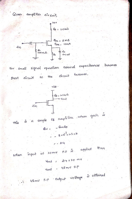
3- For amplifier circuit shown in figure. If the input voltage, Vin = 20 mV peak-peak,...
The input voltage vin t for the circuit shown is the sine curve in the graph...
 The input voltage vin t for the circuit shown is the sine curve in the graph below f R-2 k, what value must be chosen for the capacitor so that the peak to peak output amplitude is 2 V ? in(t) (V) 3 t (ms) 10 Express your answer to three signficant figures in μF View Available Hint(s) C= AF
C- Amplifier: Consider figure 3. This circuit uses the JFET to amplify the input signal voltage F...
 C- Amplifier: Consider figure 3. This circuit uses the JFET to amplify the input signal voltage First the dc operation must be set. Use equation 1 and your previous data to calculate the value of Vas required to give I-0.5 mA. Determine the source resistance Rs needed to set this bias. Set up the circuit of figure 3 with your calculated value of Rs. Measure Vo and Vs to determine if your operating conditions are correct. Apply an input voltage...
(c) Consider the circuit shown in Figure Q4c. If the input voltage is Vin = 5...
 (c) Consider the circuit shown in Figure Q4c. If the input voltage is Vin = 5 [V] and open loop gain A0 = 10,000, determine the output voltage and derive the closed-loop gain [4 marks] Page 5 of 6 Figure Q4c
Question 3 (10 marks) Calculate the input power , the output power and the efficiency of the amplifier circuit shown in Fig.(3) for an input voltage that results in a base current of 10 mA peak t...
 Question 3 (10 marks) Calculate the input power , the output power and the efficiency of the amplifier circuit shown in Fig.(3) for an input voltage that results in a base current of 10 mA peak to peak. ㄟˇㄟ Fig. (3) 25
Question 3 (10 marks) Calculate the input power , the output power and the efficiency of the amplifier circuit shown in Fig.(3) for an input voltage that results in a base current of 10 mA peak to peak....
Question 3 (10 marks) Calculate the input power , the output power and the efficiency of the amplifier circuit shown in Fig.(3) for an input voltage that results in a base current of 10 mA peak to peak. ㄟˇㄟ Fig. (3) 25
Question 3 (10 marks) Calculate the input power , the output power and the efficiency of the amplifier circuit shown in Fig.(3) for an input voltage that results in a base current of 10 mA peak to peak....
For the amplifier circuits in Figs.3 and 7: a. Write an expression for the output voltage,...
 For the amplifier circuits in Figs.3 and 7:
a. Write an expression for the output voltage, vo, in terms of
the resistor symbols and the input voltage, vin.
---For the first circuit (Fig. 3), the feedback resistor is the
series combination of R2 and R3. Use both of these resistor symbols
in your expression.
-- For circuit 2 (Fig. 7), assume that vin = 5V and ignore
potentiometer R1 and C3.
b. Using resistor values and input voltage amplitudes, calculate...
For the amplifier circuits in Figs.3 and 7:
a. Write an expression for the output voltage, vo, in terms of
the resistor symbols and the input voltage, vin.
---For the first circuit (Fig. 3), the feedback resistor is the
series combination of R2 and R3. Use both of these resistor symbols
in your expression.
-- For circuit 2 (Fig. 7), assume that vin = 5V and ignore
potentiometer R1 and C3.
b. Using resistor values and input voltage amplitudes, calculate...
A MOSFET is wired as a common-source amplifier as shown below. The input voltage vIN is...
 A MOSFET is wired as a common-source amplifier as shown below.
The input voltage vIN is the total of the source for
biasing the circuit at its operating point (vBIAS), and
a small signal ac source providing the signal that we want to
amplify (vin). The total output voltage is
vO.
a) Assume VDD = 5?, VIN = 2?, and ? = 4?Ω
in the circuit and the MOSFET parameters are K =
0.5??/?2, VTH 1?, and ? = 0.05V-1....
A MOSFET is wired as a common-source amplifier as shown below.
The input voltage vIN is the total of the source for
biasing the circuit at its operating point (vBIAS), and
a small signal ac source providing the signal that we want to
amplify (vin). The total output voltage is
vO.
a) Assume VDD = 5?, VIN = 2?, and ? = 4?Ω
in the circuit and the MOSFET parameters are K =
0.5??/?2, VTH 1?, and ? = 0.05V-1....
Q1. For the cascade amplifier circuit shown in Fig (1): a) What are the functions of the capacitors C, C2 and C3? And w...
 Q1. For the cascade amplifier circuit shown in Fig (1): a) What are the functions of the capacitors C, C2 and C3? And what are the functions of the capacitors Cs and CE? b) What are the functions of the resistors RD and Rc? c) Draw the DC biasing circuits for each stage. d) Find loa, VGsa, VDs and gm for the JFET stage (you may use either mathematical or graphical methods) e) Calculate l, Ic, le and Ve for...
In the circuit below, the input voltage is Vin-Vinegakcos(wt), R-20 ΚΩandC15nFw l. in al Show that the output voltage is VotVcos (wt-), where V-V n peak/V1 + (RC) b) Show that this result justifies c...
 In the circuit below, the input voltage is Vin-Vinegakcos(wt), R-20 ΚΩandC15nFw l. in al Show that the output voltage is VotVcos (wt-), where V-V n peak/V1 + (RC) b) Show that this result justifies calling this circuit a high-pass filter+ c) Find an expression for the phase constant δ in terms of R,C and d) At what frequency is Vi (1/V2) Vin peak? That particular frequency is known as the 3dB frequency, or f3dB, of the circuit
In the circuit...
In the circuit below, the input voltage is Vin-Vinegakcos(wt), R-20 ΚΩandC15nFw l. in al Show that the output voltage is VotVcos (wt-), where V-V n peak/V1 + (RC) b) Show that this result justifies calling this circuit a high-pass filter+ c) Find an expression for the phase constant δ in terms of R,C and d) At what frequency is Vi (1/V2) Vin peak? That particular frequency is known as the 3dB frequency, or f3dB, of the circuit
In the circuit...
c) In estimating DC imperfections (input offset voltage, input offset current and the inverting amplifier with...
 c) In estimating DC imperfections (input offset voltage, input offset current and the inverting amplifier with nominal gain of -100 using 1 current) of an op-map, an and 10MQ resistors is implemented using the op-amp as shown in Fig 2(a) below R2 10MQ R 100k Vi Vo Figure 2(a): Inverting amplifier Measurements are conducted on the output voltage of the inverting amplifier under the following conditions: (i) the input (V) is open circuited and the output voltage is found to...
1. Find the ratio of the output voltage to the input voltage, Vo/Vin, in the circuit...
 1. Find the ratio of the output voltage to the input voltage, Vo/Vin, in the circuit shown. State your assumptions in using the ideal op-amp model. 15 k2 Vin 2. Find the output voltage Vo in the circuit shown assuming an ideal op-amp. State your assumptions in using the ideal op-amp model 15 k12 Vo . Find the voltage Vx and the output voltage Vo in the circuit shown assuming ideal op-amp 3 k2 1 V 6 kn 12 k2
 The input voltage vin t for the circuit shown is the sine curve in the graph below f R-2 k, what value must be chosen for the capacitor so that the peak to peak output amplitude is 2 V ? in(t) (V) 3 t (ms) 10 Express your answer to three signficant figures in μF View Available Hint(s) C= AF
 C- Amplifier: Consider figure 3. This circuit uses the JFET to amplify the input signal voltage First the dc operation must be set. Use equation 1 and your previous data to calculate the value of Vas required to give I-0.5 mA. Determine the source resistance Rs needed to set this bias. Set up the circuit of figure 3 with your calculated value of Rs. Measure Vo and Vs to determine if your operating conditions are correct. Apply an input voltage...
 (c) Consider the circuit shown in Figure Q4c. If the input voltage is Vin = 5 [V] and open loop gain A0 = 10,000, determine the output voltage and derive the closed-loop gain [4 marks] Page 5 of 6 Figure Q4c
 Question 3 (10 marks) Calculate the input power , the output power and the efficiency of the amplifier circuit shown in Fig.(3) for an input voltage that results in a base current of 10 mA peak to peak. ㄟˇㄟ Fig. (3) 25
Question 3 (10 marks) Calculate the input power , the output power and the efficiency of the amplifier circuit shown in Fig.(3) for an input voltage that results in a base current of 10 mA peak to peak....
Question 3 (10 marks) Calculate the input power , the output power and the efficiency of the amplifier circuit shown in Fig.(3) for an input voltage that results in a base current of 10 mA peak to peak. ㄟˇㄟ Fig. (3) 25
Question 3 (10 marks) Calculate the input power , the output power and the efficiency of the amplifier circuit shown in Fig.(3) for an input voltage that results in a base current of 10 mA peak to peak....
 For the amplifier circuits in Figs.3 and 7:
a. Write an expression for the output voltage, vo, in terms of
the resistor symbols and the input voltage, vin.
---For the first circuit (Fig. 3), the feedback resistor is the
series combination of R2 and R3. Use both of these resistor symbols
in your expression.
-- For circuit 2 (Fig. 7), assume that vin = 5V and ignore
potentiometer R1 and C3.
b. Using resistor values and input voltage amplitudes, calculate...
For the amplifier circuits in Figs.3 and 7:
a. Write an expression for the output voltage, vo, in terms of
the resistor symbols and the input voltage, vin.
---For the first circuit (Fig. 3), the feedback resistor is the
series combination of R2 and R3. Use both of these resistor symbols
in your expression.
-- For circuit 2 (Fig. 7), assume that vin = 5V and ignore
potentiometer R1 and C3.
b. Using resistor values and input voltage amplitudes, calculate...
 A MOSFET is wired as a common-source amplifier as shown below.
The input voltage vIN is the total of the source for
biasing the circuit at its operating point (vBIAS), and
a small signal ac source providing the signal that we want to
amplify (vin). The total output voltage is
vO.
a) Assume VDD = 5?, VIN = 2?, and ? = 4?Ω
in the circuit and the MOSFET parameters are K =
0.5??/?2, VTH 1?, and ? = 0.05V-1....
A MOSFET is wired as a common-source amplifier as shown below.
The input voltage vIN is the total of the source for
biasing the circuit at its operating point (vBIAS), and
a small signal ac source providing the signal that we want to
amplify (vin). The total output voltage is
vO.
a) Assume VDD = 5?, VIN = 2?, and ? = 4?Ω
in the circuit and the MOSFET parameters are K =
0.5??/?2, VTH 1?, and ? = 0.05V-1....
 Q1. For the cascade amplifier circuit shown in Fig (1): a) What are the functions of the capacitors C, C2 and C3? And what are the functions of the capacitors Cs and CE? b) What are the functions of the resistors RD and Rc? c) Draw the DC biasing circuits for each stage. d) Find loa, VGsa, VDs and gm for the JFET stage (you may use either mathematical or graphical methods) e) Calculate l, Ic, le and Ve for...
 In the circuit below, the input voltage is Vin-Vinegakcos(wt), R-20 ΚΩandC15nFw l. in al Show that the output voltage is VotVcos (wt-), where V-V n peak/V1 + (RC) b) Show that this result justifies calling this circuit a high-pass filter+ c) Find an expression for the phase constant δ in terms of R,C and d) At what frequency is Vi (1/V2) Vin peak? That particular frequency is known as the 3dB frequency, or f3dB, of the circuit
In the circuit...
In the circuit below, the input voltage is Vin-Vinegakcos(wt), R-20 ΚΩandC15nFw l. in al Show that the output voltage is VotVcos (wt-), where V-V n peak/V1 + (RC) b) Show that this result justifies calling this circuit a high-pass filter+ c) Find an expression for the phase constant δ in terms of R,C and d) At what frequency is Vi (1/V2) Vin peak? That particular frequency is known as the 3dB frequency, or f3dB, of the circuit
In the circuit...
 c) In estimating DC imperfections (input offset voltage, input offset current and the inverting amplifier with nominal gain of -100 using 1 current) of an op-map, an and 10MQ resistors is implemented using the op-amp as shown in Fig 2(a) below R2 10MQ R 100k Vi Vo Figure 2(a): Inverting amplifier Measurements are conducted on the output voltage of the inverting amplifier under the following conditions: (i) the input (V) is open circuited and the output voltage is found to...
 1. Find the ratio of the output voltage to the input voltage, Vo/Vin, in the circuit shown. State your assumptions in using the ideal op-amp model. 15 k2 Vin 2. Find the output voltage Vo in the circuit shown assuming an ideal op-amp. State your assumptions in using the ideal op-amp model 15 k12 Vo . Find the voltage Vx and the output voltage Vo in the circuit shown assuming ideal op-amp 3 k2 1 V 6 kn 12 k2
Most questions answered within 3 hours.
-
among the three different ways to link CSS specifications to an
HTML document (inline CSS, document...
asked 8 minutes ago -
(1) Write the net ionic equation for the reaction that occurs
when equal volumes of 0.191...
asked 35 minutes ago -
On the night of April 18, 1775, a signal was to be sent from the
Old...
asked 18 minutes ago -
For each of the following strong base solutions, determine
[OH−],[H3O+], pH, and pOH 4.8 x 10^-4...
asked 14 minutes ago -
The magnitude of the electric field inside a capacitor is 6.6 x
106 N/C. What is...
asked 14 minutes ago -
Organizations may have only a few products or many products in a
product line. Consider Campbell...
asked 27 minutes ago -
could you please help me to explain the nmr splitting
integration and chemical shift and assignment...
asked 23 minutes ago -
A
29.0 cm diameter coil consists of 23 turns of cylindrical copper
wire 2.00 mm in...
asked 29 minutes ago -
Q1
Two of your friends each received the results of their
first midterm exam this term....
asked 46 minutes ago -
A 0.500-kg object, suspended from an ideal spring of spring
constant 30.2 N/m, is oscillating vertically....
asked 44 minutes ago -
Please help and show work. I keep getting the wrong answers for
these problems
1. Cell...
asked 42 minutes ago -
If there is a SNP in the read with respect to the
reference genome, how would a...
asked 44 minutes ago