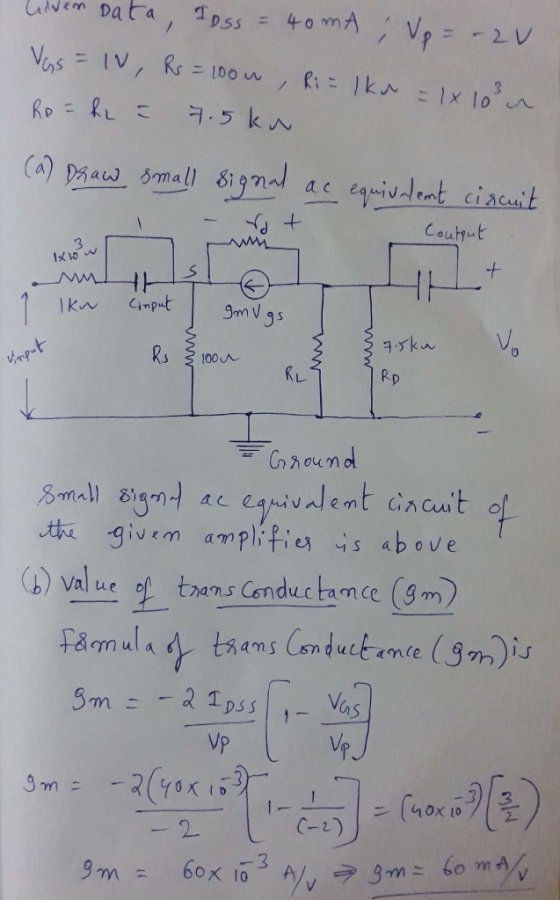
![Note: Question 1 is to be done outside the lab hours] A JFET common gate amplifier circuit is shown in Figure la. The supply voltage is 15V. The JFET has the following parameters which are: lss 40mA and Vp2V. The JFET is biased at VGs IV The resistors have the following values: Rs = 100Q, R. = 1 k? and RD-R,-7.5k(2. +15V out Output Cin Ri nput Fig. la (a Draw the small signal ac equivalent circuit of this amplifier (b) Calculate the value of the transconductance. (c Calculate the small-signal voltage gain of this amplifier (d) Calculate the high cut-off frequency at the input side. (e Calculate the high cut-off frequency at the output side. ( Determine the dominant pole frequency of this amplifier](http://img.homeworklib.com/questions/db1988f0-13f1-11ec-b811-a9b3eb02fe05.png?x-oss-process=image/resize,w_560)
analog electronic question.. please answer all by showing step by step calculation clearly. tq
Homework Answers
Add Answer to:
analog electronic question.. please answer all by
showing step by step calculation clearly. tq
Note: Question...
1-Clear handwriting 2-Correct answer 3-Organized 4-answer all the questions Please Problem 2 On the circuit on...
 1-Clear handwriting
2-Correct answer
3-Organized
4-answer all the questions
Please
Problem 2 On the circuit on Figure P2, transi stor Q1 has a threshold voltage of Vt = 2 V and a transconductance parameter of k = 100 mA/V2. Note that Vcc = -Vee = 4.5 V. Moreover, capacitors C1, C2, and C3 can be assumed to be very large VDD 4.5.0 R3 25kQ R1 300kn C2 Vout C1 Rsig Q1 1k0 R2 200kn Vsig (R4 2kQ C3 -4.5V VSS...
1-Clear handwriting
2-Correct answer
3-Organized
4-answer all the questions
Please
Problem 2 On the circuit on Figure P2, transi stor Q1 has a threshold voltage of Vt = 2 V and a transconductance parameter of k = 100 mA/V2. Note that Vcc = -Vee = 4.5 V. Moreover, capacitors C1, C2, and C3 can be assumed to be very large VDD 4.5.0 R3 25kQ R1 300kn C2 Vout C1 Rsig Q1 1k0 R2 200kn Vsig (R4 2kQ C3 -4.5V VSS...
QUESTION 1 Anna the Audiophile has asked for your help to build an amplifier and filter...
 QUESTION 1 Anna the Audiophile has asked for your help to build an amplifier and filter to take small signals from her hifi system and amplify them so that she can drive her new subwoofer. The hifi system produces AC signals at varying frequencies with 250mVrms maximum magnitude Her subwoofer requires the signals to be 20 Vrms maximum magnitude. The signals that Anna is interested in are below 200 Hz. She would like the filter to attenuate signals at frequencies...
Could you please show me how I can drw those circuits. please using (NI Multisim 14)...
 Could you please show me how I can drw those circuits.
please using (NI Multisim 14)
Optocoupler Objectives Use an ohmmeter to determine the condition of the optoisolator. Observe the operation of an optocoupler. Determine the maximum frequency response of the optocoupler. Required Materials (1) Dual DC power supply (1) Function generator (1) Oscilloscope (2) Multimeters (1) Optocoupler (ECG3040) (1) 3.9ΚΩ resistor (1) 220 resistor Introduction An optoisolator is a hybrid integrated circuit that contains an LED on one side...
Could you please show me how I can drw those circuits.
please using (NI Multisim 14)
Optocoupler Objectives Use an ohmmeter to determine the condition of the optoisolator. Observe the operation of an optocoupler. Determine the maximum frequency response of the optocoupler. Required Materials (1) Dual DC power supply (1) Function generator (1) Oscilloscope (2) Multimeters (1) Optocoupler (ECG3040) (1) 3.9ΚΩ resistor (1) 220 resistor Introduction An optoisolator is a hybrid integrated circuit that contains an LED on one side...
Please answer all the parts of the question clearly and fully! Thank you! Numerical Answers: (b)...
 Please answer all the parts of the question clearly and fully!
Thank you!
Numerical Answers:
(b) (0.0 A, 24 V), (approximately 1.6 A, 0.32 V)
(c) 38.4 W, 0.5 W
(e) 0.26 W + 1.5 mW
SECTION B: Attempt any Two) questions 150 marks total! Q3 A MOSFET is used as a low-side switch to control a 15 2 resistive load from a 24 supply. The MOSFET has RDSan VDC 0.2 ? and ton-tof-40 ns. (a) Draw a suitable circuit....
Please answer all the parts of the question clearly and fully!
Thank you!
Numerical Answers:
(b) (0.0 A, 24 V), (approximately 1.6 A, 0.32 V)
(c) 38.4 W, 0.5 W
(e) 0.26 W + 1.5 mW
SECTION B: Attempt any Two) questions 150 marks total! Q3 A MOSFET is used as a low-side switch to control a 15 2 resistive load from a 24 supply. The MOSFET has RDSan VDC 0.2 ? and ton-tof-40 ns. (a) Draw a suitable circuit....
Yes, this is one problem. Please solve ALL PARTS. Guaranteed thumbs up for the person who solves it. 3 1. Photodiode...
 Yes, this is one problem. Please solve ALL PARTS. Guaranteed
thumbs up for the person who solves it.
3 1. Photodiode amplifier circuit You are designinga CF photosensor circuit for a light detection and ranging LiDAR) system in autonomous vehicles. The circuit utilizes a transimpedance amplifier to convert low-level RF photodiode current signal to a usable voltage output. It consists of a photodiode, an amplifier, and feedback capacitor/resistor pair as shown in Figure 1. We will derive simple equations to...
Yes, this is one problem. Please solve ALL PARTS. Guaranteed
thumbs up for the person who solves it.
3 1. Photodiode amplifier circuit You are designinga CF photosensor circuit for a light detection and ranging LiDAR) system in autonomous vehicles. The circuit utilizes a transimpedance amplifier to convert low-level RF photodiode current signal to a usable voltage output. It consists of a photodiode, an amplifier, and feedback capacitor/resistor pair as shown in Figure 1. We will derive simple equations to...
Problem 3: Design Problem On Figure P3a, you have a Common Source (CS) n-channel MOSFET amplifier....
 Problem 3: Design Problem On Figure P3a, you have a Common Source (CS) n-channel MOSFET amplifier. Notice the absence of a source resistor Rsig and load resistor R. If we know how the present amplifier (the one on Figure P3a) behaves without Rsig and RL, we can infer its behaviors if Rsig and R were to be added. design the amplifier circuit on Figure P3a, i.e., you have to find appropriate values for RGj You are to RG,, RD, and...
 1-Clear handwriting
2-Correct answer
3-Organized
4-answer all the questions
Please
Problem 2 On the circuit on Figure P2, transi stor Q1 has a threshold voltage of Vt = 2 V and a transconductance parameter of k = 100 mA/V2. Note that Vcc = -Vee = 4.5 V. Moreover, capacitors C1, C2, and C3 can be assumed to be very large VDD 4.5.0 R3 25kQ R1 300kn C2 Vout C1 Rsig Q1 1k0 R2 200kn Vsig (R4 2kQ C3 -4.5V VSS...
1-Clear handwriting
2-Correct answer
3-Organized
4-answer all the questions
Please
Problem 2 On the circuit on Figure P2, transi stor Q1 has a threshold voltage of Vt = 2 V and a transconductance parameter of k = 100 mA/V2. Note that Vcc = -Vee = 4.5 V. Moreover, capacitors C1, C2, and C3 can be assumed to be very large VDD 4.5.0 R3 25kQ R1 300kn C2 Vout C1 Rsig Q1 1k0 R2 200kn Vsig (R4 2kQ C3 -4.5V VSS...
 QUESTION 1 Anna the Audiophile has asked for your help to build an amplifier and filter to take small signals from her hifi system and amplify them so that she can drive her new subwoofer. The hifi system produces AC signals at varying frequencies with 250mVrms maximum magnitude Her subwoofer requires the signals to be 20 Vrms maximum magnitude. The signals that Anna is interested in are below 200 Hz. She would like the filter to attenuate signals at frequencies...
 Could you please show me how I can drw those circuits.
please using (NI Multisim 14)
Optocoupler Objectives Use an ohmmeter to determine the condition of the optoisolator. Observe the operation of an optocoupler. Determine the maximum frequency response of the optocoupler. Required Materials (1) Dual DC power supply (1) Function generator (1) Oscilloscope (2) Multimeters (1) Optocoupler (ECG3040) (1) 3.9ΚΩ resistor (1) 220 resistor Introduction An optoisolator is a hybrid integrated circuit that contains an LED on one side...
Could you please show me how I can drw those circuits.
please using (NI Multisim 14)
Optocoupler Objectives Use an ohmmeter to determine the condition of the optoisolator. Observe the operation of an optocoupler. Determine the maximum frequency response of the optocoupler. Required Materials (1) Dual DC power supply (1) Function generator (1) Oscilloscope (2) Multimeters (1) Optocoupler (ECG3040) (1) 3.9ΚΩ resistor (1) 220 resistor Introduction An optoisolator is a hybrid integrated circuit that contains an LED on one side...
 Please answer all the parts of the question clearly and fully!
Thank you!
Numerical Answers:
(b) (0.0 A, 24 V), (approximately 1.6 A, 0.32 V)
(c) 38.4 W, 0.5 W
(e) 0.26 W + 1.5 mW
SECTION B: Attempt any Two) questions 150 marks total! Q3 A MOSFET is used as a low-side switch to control a 15 2 resistive load from a 24 supply. The MOSFET has RDSan VDC 0.2 ? and ton-tof-40 ns. (a) Draw a suitable circuit....
Please answer all the parts of the question clearly and fully!
Thank you!
Numerical Answers:
(b) (0.0 A, 24 V), (approximately 1.6 A, 0.32 V)
(c) 38.4 W, 0.5 W
(e) 0.26 W + 1.5 mW
SECTION B: Attempt any Two) questions 150 marks total! Q3 A MOSFET is used as a low-side switch to control a 15 2 resistive load from a 24 supply. The MOSFET has RDSan VDC 0.2 ? and ton-tof-40 ns. (a) Draw a suitable circuit....
 Yes, this is one problem. Please solve ALL PARTS. Guaranteed
thumbs up for the person who solves it.
3 1. Photodiode amplifier circuit You are designinga CF photosensor circuit for a light detection and ranging LiDAR) system in autonomous vehicles. The circuit utilizes a transimpedance amplifier to convert low-level RF photodiode current signal to a usable voltage output. It consists of a photodiode, an amplifier, and feedback capacitor/resistor pair as shown in Figure 1. We will derive simple equations to...
Yes, this is one problem. Please solve ALL PARTS. Guaranteed
thumbs up for the person who solves it.
3 1. Photodiode amplifier circuit You are designinga CF photosensor circuit for a light detection and ranging LiDAR) system in autonomous vehicles. The circuit utilizes a transimpedance amplifier to convert low-level RF photodiode current signal to a usable voltage output. It consists of a photodiode, an amplifier, and feedback capacitor/resistor pair as shown in Figure 1. We will derive simple equations to...
 Problem 3: Design Problem On Figure P3a, you have a Common Source (CS) n-channel MOSFET amplifier. Notice the absence of a source resistor Rsig and load resistor R. If we know how the present amplifier (the one on Figure P3a) behaves without Rsig and RL, we can infer its behaviors if Rsig and R were to be added. design the amplifier circuit on Figure P3a, i.e., you have to find appropriate values for RGj You are to RG,, RD, and...
Most questions answered within 3 hours.
-
Suppose that XX is a random variable with mean 16 and standard
deviation 5 . Also...
asked 29 minutes ago -
Calculate the number density of argon gas at a temperature of
24C and a pressure of...
asked 3 hours ago -
Alternative
Classification
How to Estimate
Probabilities from Data? ( For continuous Attributes)
And How to generate...
asked 3 hours ago -
An explosion breaks a 20.0-kg object into three parts. The
object is initially moving at a...
asked 4 hours ago -
Calculate the approximate number of residues of Rubisco, which
is involved in carbon fixation in plants,...
asked 5 hours ago -
Other decisions about scientific claims can have a much broader
impact.ENERGYarrow-10x10.png, environment, health, security - all...
asked 6 hours ago -
I need to write a research paper and work cited about this
topic: The United States...
asked 6 hours ago -
Hello! I was wondering if I could have some help?
If the vapor pressure of carvone...
asked 7 hours ago -
An economist wants to estimate the mean per capita income (in
thousands of dollars) for a...
asked 7 hours ago -
What would be the input/output characteristic of a circuit
obtained by putting two of your 2's-complementers...
asked 7 hours ago -
In Drosophila, the transition from the syncytial blastoderm
stage to the cellular blastoderm stage is a...
asked 8 hours ago -
Project management question:
Name 3 different types of resources (hint: humans are one
type)
asked 8 hours ago