

Homework Answers
First we revisit the problem 2.6 whose analysis is as follows :


To obtain better voltage regulation in shunt regulator, the zener diode can be connected to the base circuit of a power transistor
as shown in the figure : 
This configuration reduces the current flow in the diode. The power transistor used in this configuration is known as pass transistor. The purpose of CL is to ensure that the variations in one of the regulated power supply loads will not be fed to other loads. That is, the capacitor effectively shorts out high-frequency variations.
Because of the current amplifying property of the transistor, the current in the zener diode is small. Hence there is little voltage drop across the diode resistance, and the zener approximates an ideal constant voltage source.
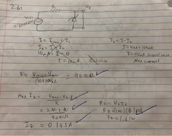
The current through resistor R is the sum of zener current IZ and the transistor base current IB ( = IL / β ).
IL = IZ + IB
The output voltage across RL resistance is given by
VO = VZ – VBE
Where VBE » 0.7 V
Therefore, VO= constant.
The emitter current is same as load current. The current IR is assumed to be constant for a given supply voltage. Therefore, if IL increases, it needs more base currents, to increase base current Iz decreases. The difference in this regulator with zener regulator is that in later case the zener current decreases (increase) by same amount by which the load current increases (decreases). Thus the current range is less, while in the shunt regulators, if IL increases by ΔIL then IB should increase by ΔIL / β or IZ should decrease by ΔIL / β. Therefore the current range control is more for the same rating zener.
NOTE : HERE SOURCE RESISTANCE IS NOT MENTIONED IN THE QUESTION ,
SO WE NEGLECT IT.
The simplified circuit of the shunt regulator is shown in the above figure .
Now we analyse the modified scheme :


Add Answer to:
im having trouble with exercise 2.7. It requires info from 2.6
so I have posted 2.6...
Most questions answered within 3 hours.
-
1. Which region has taken the lead in the world of
e-waste handling?
a) European Union...
asked 2 minutes ago -
If you’re standing at the bottom of a hill and asked to evaluate
it while being...
asked 8 minutes ago -
A 8.15- g bullet from a 9-mm pistol has a velocity of 366.0 m/s.
It strikes...
asked 1 hour ago -
The outstanding bonds of Alpha Extracts have a yield to maturity
of 7.4 percent and a...
asked 1 hour ago -
The Problem: The Case of the Harmonizing Vacations
Your CEO is exploring partnering with a European...
asked 2 hours ago -
A chemical equation is balanced by adding coefficients in front
of some formulas so that the...
asked 2 hours ago -
From the literature (reference your sources): What are the
lattice parameters of calcite and aragonite? Why...
asked 3 hours ago -
Your system is rejecting the question am asking which is
preceded by a case study. It...
asked 3 hours ago -
3. On January 2, 2000, Larry creates a trust with himself as
trustee. Larry as trustee...
asked 3 hours ago -
A member of the volleyball team spikes the ball. During this
process, she changes the velocity...
asked 3 hours ago -
Are adult gamers less likely to use a gaming console (Xbox,
PlayStation, Wii, etc...) than teen...
asked 4 hours ago -
The University of
Texas recently reported that 43% of college students aged 18-24
would spend their...
asked 4 hours ago