1. Draw a circuit diagram that implements the logic for a two-input OR gate that lights...
1. Draw a circuit diagram that implements the logic for a two-input OR gate that lights an LED when the OR gate is asserted. Use only NPN transistors, resistors, jumper wires for the inputs, a power source, and an LED.
Homework Answers
OR gate: If one input is high or both the inputs are high the OR gate gives the output as high.
To implement OR logic using transistors, we need to connect the transistors in series
Collectors of transistors are connected to each other and the first transistor is also connected to the power source.
The emitters are given as input to the LED.
The base of each transistor is connected to a resistor and from there we give the input A, B.
Truth Table for OR logic:
| A | B | A OR B |
| 0 | 0 | 0 |
| 0 | 1 | 1 |
| 1 | 0 | 1 |
| 1 | 1 | 1 |
Circuit Diagram: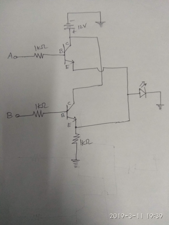
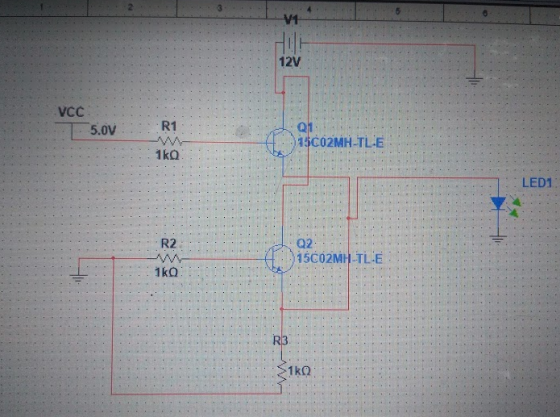
When we implement the above circuit and give the inputs, we get the corresponding output at the LED.
Simulation:
Add Answer to:
1. Draw a circuit diagram that implements the logic for a
two-input OR gate that lights...
Write the Boolean expression and draw the gate logic diagram and typical PLC ladder logic dia- gr...
 Write the Boolean expression and draw the gate logic diagram and typical PLC ladder logic dia- gram for a control system wherein a fan is to run only when all of the following conditions are met: . Input A is OFF . Input B is ON or input C is ON, or both B and C 5. are ON Inputs D and E are both ON One or more of inputs F, G, or H are ON 4. Express each...
The layout of a CMOS complex logic circuit is given in the Figure 1. 1. Draw the corresponding circuit diagram; and a....
 The layout of a CMOS complex logic circuit is given in the Figure 1. 1. Draw the corresponding circuit diagram; and a. b. Calculate the (W/equivaientfall the nMOS and PMOS transistors for simultaneous equivalent switching of all the inputs, assuming that (W/L), = 25 for all pMOS transistors and W-20 for all nMOS transistors F(A,B,C,D,E ) A B Figure 1
The layout of a CMOS complex logic circuit is given in the Figure 1. 1. Draw the corresponding circuit diagram;...
The layout of a CMOS complex logic circuit is given in the Figure 1. 1. Draw the corresponding circuit diagram; and a. b. Calculate the (W/equivaientfall the nMOS and PMOS transistors for simultaneous equivalent switching of all the inputs, assuming that (W/L), = 25 for all pMOS transistors and W-20 for all nMOS transistors F(A,B,C,D,E ) A B Figure 1
The layout of a CMOS complex logic circuit is given in the Figure 1. 1. Draw the corresponding circuit diagram;...
Draw a combinational logic circuit that implements a four-channel multiplexer which uses two input lines to...
Draw a combinational logic circuit that implements a four-channel multiplexer which uses two input lines to select the input channel to be connected to the output.
a) Design a CMOS logic gate that implements the logic function Y = AB+(CD+E) if the...
 a) Design a CMOS logic gate that implements the logic function Y = AB+(CD+E) if the reference inverter has (WIL)n = 2/1, (W/L)= 5/1 b) What is the equivalent W/L for the NMOS section when all transistors are ON?
Please with details and explanations The layout of a CMOS complex logic circuit is given in the Figure 1. 4. (10 Marks) Draw the corresponding circuit diagram; and cdlculate the (equivaent of all...
 Please with details and explanations
The layout of a CMOS complex logic circuit is given in the Figure 1. 4. (10 Marks) Draw the corresponding circuit diagram; and cdlculate the (equivaent of all the nMOS and PMOS transistors for simultaneous switching of all the inputs, assuming that (W/L)p = 15 for all pMOS transistors and (w/2), a. 5 for all nMOS (10 Marks) transistors Vdd PMOS IL NMOS Figure 1
The layout of a CMOS complex logic circuit is given...
Please with details and explanations
The layout of a CMOS complex logic circuit is given in the Figure 1. 4. (10 Marks) Draw the corresponding circuit diagram; and cdlculate the (equivaent of all the nMOS and PMOS transistors for simultaneous switching of all the inputs, assuming that (W/L)p = 15 for all pMOS transistors and (w/2), a. 5 for all nMOS (10 Marks) transistors Vdd PMOS IL NMOS Figure 1
The layout of a CMOS complex logic circuit is given...
The layout of a CMOS complex logic circuit is given in the Figure 1. 4. Draw the corresponding circuit diagram; and (10 Marks) a. b. Colculate the W/Doivalent of all the nMOS and PMOS transistors...
 The layout of a CMOS complex logic circuit is given in the Figure 1. 4. Draw the corresponding circuit diagram; and (10 Marks) a. b. Colculate the W/Doivalent of all the nMOS and PMOS transistors for simultaneous switching of all the inputs, assuming that (W/, 25 for all MOS transistors and (W/, 20 for al nMOS transistors. (10 Marks) FIA, B,C,D,E ) A B Figure 1
The layout of a CMOS complex logic circuit is given in the Figure 1....
The layout of a CMOS complex logic circuit is given in the Figure 1. 4. Draw the corresponding circuit diagram; and (10 Marks) a. b. Colculate the W/Doivalent of all the nMOS and PMOS transistors for simultaneous switching of all the inputs, assuming that (W/, 25 for all MOS transistors and (W/, 20 for al nMOS transistors. (10 Marks) FIA, B,C,D,E ) A B Figure 1
The layout of a CMOS complex logic circuit is given in the Figure 1....
The layout of a CMOS complex logic circuit is given in the Figure 1. Draw the corresponding circuit diagram; and Calcula...
 The layout of a CMOS complex logic circuit is given in the
Figure 1. Draw the corresponding circuit diagram; and
Calculate the (W⁄L)_equivalent of all the nMOS and PMOS
transistors for simultaneous switching of all the inputs, assuming
that (W⁄L)p =20 for all pMOS transistors and (W⁄L)n =15 for all
nMOS transistors.
Windows VDD poly silicon n+ diffussion OUT P+ diffusion Centact GND
Windows VDD poly silicon n+ diffussion OUT P+ diffusion Centact GND
The layout of a CMOS complex logic circuit is given in the
Figure 1. Draw the corresponding circuit diagram; and
Calculate the (W⁄L)_equivalent of all the nMOS and PMOS
transistors for simultaneous switching of all the inputs, assuming
that (W⁄L)p =20 for all pMOS transistors and (W⁄L)n =15 for all
nMOS transistors.
Windows VDD poly silicon n+ diffussion OUT P+ diffusion Centact GND
Windows VDD poly silicon n+ diffussion OUT P+ diffusion Centact GND
(a) The circuit shown below in Figure 3 has a two-input logic gate hidden from view....
 (a) The circuit shown below in Figure 3 has a two-input logic gate hidden from view. By inspection of the output function F, identify the hidden logic gate. ; hidden logic F-(ADB)(C08) gate cas Figure 3 (b) Draw a truth table for the function F given in part (a) above and hence derive an alternative 'sum of products' expression for F.
3. Design the CMOS gate that implements the following function OUT- AB (a) Draw the circuit schematic without any output inverter. (b) Size all the transistors in this circuit such that TR 3Tr. The m...
 3. Design the CMOS gate that implements the following function OUT- AB (a) Draw the circuit schematic without any output inverter. (b) Size all the transistors in this circuit such that TR 3Tr. The minimum geometry is W.
3. Design the CMOS gate that implements the following function OUT- AB (a) Draw the circuit schematic without any output inverter. (b) Size all the transistors in this circuit such that TR 3Tr. The minimum geometry is W.
3. Design the CMOS gate that implements the following function OUT- AB (a) Draw the circuit schematic without any output inverter. (b) Size all the transistors in this circuit such that TR 3Tr. The minimum geometry is W.
The layout of a CMOS complex logic circuit is given in the Figure 1 4. Draw the corresponding circuit diagram; and (10 Marks) a. b. Calculate the (W) of all the nMOS and PMOS transistors for simul...
 The layout of a CMOS complex logic circuit is given in the Figure 1 4. Draw the corresponding circuit diagram; and (10 Marks) a. b. Calculate the (W) of all the nMOS and PMOS transistors for simultaneous switching (W/), 15 for all of all the inputs, assuming that (Wh),-20 for all pMOS transistors and (w/L), = 15 for all (WL 20 for all pMOS transistors and (10 Marks) nMOS transistors VDD n well metal poly silicon n+ diffussion OUT Contact...
 Write the Boolean expression and draw the gate logic diagram and typical PLC ladder logic dia- gram for a control system wherein a fan is to run only when all of the following conditions are met: . Input A is OFF . Input B is ON or input C is ON, or both B and C 5. are ON Inputs D and E are both ON One or more of inputs F, G, or H are ON 4. Express each...
 The layout of a CMOS complex logic circuit is given in the Figure 1. 1. Draw the corresponding circuit diagram; and a. b. Calculate the (W/equivaientfall the nMOS and PMOS transistors for simultaneous equivalent switching of all the inputs, assuming that (W/L), = 25 for all pMOS transistors and W-20 for all nMOS transistors F(A,B,C,D,E ) A B Figure 1
The layout of a CMOS complex logic circuit is given in the Figure 1. 1. Draw the corresponding circuit diagram;...
The layout of a CMOS complex logic circuit is given in the Figure 1. 1. Draw the corresponding circuit diagram; and a. b. Calculate the (W/equivaientfall the nMOS and PMOS transistors for simultaneous equivalent switching of all the inputs, assuming that (W/L), = 25 for all pMOS transistors and W-20 for all nMOS transistors F(A,B,C,D,E ) A B Figure 1
The layout of a CMOS complex logic circuit is given in the Figure 1. 1. Draw the corresponding circuit diagram;...
 a) Design a CMOS logic gate that implements the logic function Y = AB+(CD+E) if the reference inverter has (WIL)n = 2/1, (W/L)= 5/1 b) What is the equivalent W/L for the NMOS section when all transistors are ON?
 Please with details and explanations
The layout of a CMOS complex logic circuit is given in the Figure 1. 4. (10 Marks) Draw the corresponding circuit diagram; and cdlculate the (equivaent of all the nMOS and PMOS transistors for simultaneous switching of all the inputs, assuming that (W/L)p = 15 for all pMOS transistors and (w/2), a. 5 for all nMOS (10 Marks) transistors Vdd PMOS IL NMOS Figure 1
The layout of a CMOS complex logic circuit is given...
Please with details and explanations
The layout of a CMOS complex logic circuit is given in the Figure 1. 4. (10 Marks) Draw the corresponding circuit diagram; and cdlculate the (equivaent of all the nMOS and PMOS transistors for simultaneous switching of all the inputs, assuming that (W/L)p = 15 for all pMOS transistors and (w/2), a. 5 for all nMOS (10 Marks) transistors Vdd PMOS IL NMOS Figure 1
The layout of a CMOS complex logic circuit is given...
 The layout of a CMOS complex logic circuit is given in the Figure 1. 4. Draw the corresponding circuit diagram; and (10 Marks) a. b. Colculate the W/Doivalent of all the nMOS and PMOS transistors for simultaneous switching of all the inputs, assuming that (W/, 25 for all MOS transistors and (W/, 20 for al nMOS transistors. (10 Marks) FIA, B,C,D,E ) A B Figure 1
The layout of a CMOS complex logic circuit is given in the Figure 1....
The layout of a CMOS complex logic circuit is given in the Figure 1. 4. Draw the corresponding circuit diagram; and (10 Marks) a. b. Colculate the W/Doivalent of all the nMOS and PMOS transistors for simultaneous switching of all the inputs, assuming that (W/, 25 for all MOS transistors and (W/, 20 for al nMOS transistors. (10 Marks) FIA, B,C,D,E ) A B Figure 1
The layout of a CMOS complex logic circuit is given in the Figure 1....
 The layout of a CMOS complex logic circuit is given in the
Figure 1. Draw the corresponding circuit diagram; and
Calculate the (W⁄L)_equivalent of all the nMOS and PMOS
transistors for simultaneous switching of all the inputs, assuming
that (W⁄L)p =20 for all pMOS transistors and (W⁄L)n =15 for all
nMOS transistors.
Windows VDD poly silicon n+ diffussion OUT P+ diffusion Centact GND
Windows VDD poly silicon n+ diffussion OUT P+ diffusion Centact GND
The layout of a CMOS complex logic circuit is given in the
Figure 1. Draw the corresponding circuit diagram; and
Calculate the (W⁄L)_equivalent of all the nMOS and PMOS
transistors for simultaneous switching of all the inputs, assuming
that (W⁄L)p =20 for all pMOS transistors and (W⁄L)n =15 for all
nMOS transistors.
Windows VDD poly silicon n+ diffussion OUT P+ diffusion Centact GND
Windows VDD poly silicon n+ diffussion OUT P+ diffusion Centact GND
 (a) The circuit shown below in Figure 3 has a two-input logic gate hidden from view. By inspection of the output function F, identify the hidden logic gate. ; hidden logic F-(ADB)(C08) gate cas Figure 3 (b) Draw a truth table for the function F given in part (a) above and hence derive an alternative 'sum of products' expression for F.
 3. Design the CMOS gate that implements the following function OUT- AB (a) Draw the circuit schematic without any output inverter. (b) Size all the transistors in this circuit such that TR 3Tr. The minimum geometry is W.
3. Design the CMOS gate that implements the following function OUT- AB (a) Draw the circuit schematic without any output inverter. (b) Size all the transistors in this circuit such that TR 3Tr. The minimum geometry is W.
3. Design the CMOS gate that implements the following function OUT- AB (a) Draw the circuit schematic without any output inverter. (b) Size all the transistors in this circuit such that TR 3Tr. The minimum geometry is W.
 The layout of a CMOS complex logic circuit is given in the Figure 1 4. Draw the corresponding circuit diagram; and (10 Marks) a. b. Calculate the (W) of all the nMOS and PMOS transistors for simultaneous switching (W/), 15 for all of all the inputs, assuming that (Wh),-20 for all pMOS transistors and (w/L), = 15 for all (WL 20 for all pMOS transistors and (10 Marks) nMOS transistors VDD n well metal poly silicon n+ diffussion OUT Contact...
Most questions answered within 3 hours.
-
You purchase your daily coffee at the Chemist’s Coffeehouse and
have a choice of two cups:...
asked 32 minutes ago -
Which of the following pairs of chemicals could be used to make
a buffer solution?
A.)...
asked 19 minutes ago -
Problem 16-51 Sales
Activity Variance (LO 16-3)Odessa, Inc., reports the following
information concerning operations for the...
asked 57 minutes ago -
Pictured on the right are thee point charges Q1 = 18.4 μC, Q2 =
-30.6 μC,...
asked 59 minutes ago -
A graduate student is conducting research in psychology and
needs to obtain the IQ scores of...
asked 1 hour ago -
R2.84: There are 2 defective products in a production lot of 10.
An inspector randomly selected...
asked 2 hours ago -
Consider the following equilibrium system: COCl2(g) CO(g) +
Cl2(g) A 10.00 L evacuated flask is filled...
asked 3 hours ago -
1) What are the two distinct steps that one needs to perform
when developing a data...
asked 3 hours ago -
2) Write a C++ program that uses a class called “Degree” to
obtain the trigonometric
values...
asked 4 hours ago -
1. In eukaryotic cells the genomes of
&
asked 4 hours ago -
The standard enthalpy of propanol (C3H7OH) is -303.0 kJ/mol.
Compute both of the
gross and net...
asked 4 hours ago -
Why PWM using H-bridge for control motor speed is more power
effiecient than the linear amplifier...
asked 4 hours ago