
Homework Answers


Add Answer to:
The layout of a CMOS complex logic circuit is given in the Figure 1. 1. Draw the corresponding circuit diagram; and a....
Please with details and explanations The layout of a CMOS complex logic circuit is given in the Figure 1. 4. (10 Marks) Draw the corresponding circuit diagram; and cdlculate the (equivaent of all...
 Please with details and explanations
The layout of a CMOS complex logic circuit is given in the Figure 1. 4. (10 Marks) Draw the corresponding circuit diagram; and cdlculate the (equivaent of all the nMOS and PMOS transistors for simultaneous switching of all the inputs, assuming that (W/L)p = 15 for all pMOS transistors and (w/2), a. 5 for all nMOS (10 Marks) transistors Vdd PMOS IL NMOS Figure 1
The layout of a CMOS complex logic circuit is given...
Please with details and explanations
The layout of a CMOS complex logic circuit is given in the Figure 1. 4. (10 Marks) Draw the corresponding circuit diagram; and cdlculate the (equivaent of all the nMOS and PMOS transistors for simultaneous switching of all the inputs, assuming that (W/L)p = 15 for all pMOS transistors and (w/2), a. 5 for all nMOS (10 Marks) transistors Vdd PMOS IL NMOS Figure 1
The layout of a CMOS complex logic circuit is given...
The layout of a CMOS complex logic circuit is given in the Figure 1. 4. Draw the corresponding circuit diagram; and (10 Marks) a. b. Colculate the W/Doivalent of all the nMOS and PMOS transistors...
 The layout of a CMOS complex logic circuit is given in the Figure 1. 4. Draw the corresponding circuit diagram; and (10 Marks) a. b. Colculate the W/Doivalent of all the nMOS and PMOS transistors for simultaneous switching of all the inputs, assuming that (W/, 25 for all MOS transistors and (W/, 20 for al nMOS transistors. (10 Marks) FIA, B,C,D,E ) A B Figure 1
The layout of a CMOS complex logic circuit is given in the Figure 1....
The layout of a CMOS complex logic circuit is given in the Figure 1. 4. Draw the corresponding circuit diagram; and (10 Marks) a. b. Colculate the W/Doivalent of all the nMOS and PMOS transistors for simultaneous switching of all the inputs, assuming that (W/, 25 for all MOS transistors and (W/, 20 for al nMOS transistors. (10 Marks) FIA, B,C,D,E ) A B Figure 1
The layout of a CMOS complex logic circuit is given in the Figure 1....
The layout of a CMOS complex logic circuit is given in the Figure 1 4. Draw the corresponding circuit diagram; and (10 Marks) a. b. Calculate the (W) of all the nMOS and PMOS transistors for simul...
 The layout of a CMOS complex logic circuit is given in the Figure 1 4. Draw the corresponding circuit diagram; and (10 Marks) a. b. Calculate the (W) of all the nMOS and PMOS transistors for simultaneous switching (W/), 15 for all of all the inputs, assuming that (Wh),-20 for all pMOS transistors and (w/L), = 15 for all (WL 20 for all pMOS transistors and (10 Marks) nMOS transistors VDD n well metal poly silicon n+ diffussion OUT Contact...
The layout of a CMOS complex logic circuit is given in the Figure 1. Draw the corresponding circuit diagram; and Calcula...
 The layout of a CMOS complex logic circuit is given in the
Figure 1. Draw the corresponding circuit diagram; and
Calculate the (W⁄L)_equivalent of all the nMOS and PMOS
transistors for simultaneous switching of all the inputs, assuming
that (W⁄L)p =20 for all pMOS transistors and (W⁄L)n =15 for all
nMOS transistors.
Windows VDD poly silicon n+ diffussion OUT P+ diffusion Centact GND
Windows VDD poly silicon n+ diffussion OUT P+ diffusion Centact GND
The layout of a CMOS complex logic circuit is given in the
Figure 1. Draw the corresponding circuit diagram; and
Calculate the (W⁄L)_equivalent of all the nMOS and PMOS
transistors for simultaneous switching of all the inputs, assuming
that (W⁄L)p =20 for all pMOS transistors and (W⁄L)n =15 for all
nMOS transistors.
Windows VDD poly silicon n+ diffussion OUT P+ diffusion Centact GND
Windows VDD poly silicon n+ diffussion OUT P+ diffusion Centact GND
with details and explanations 4. The layout of a CMOS complex logic circuit is eiven in the Figure 1 (10 Marks) Calculate the (/equvalent of all the nMoS and PMOS transistors for simultaneous swit...
 with details and explanations
4. The layout of a CMOS complex logic circuit is eiven in the Figure 1 (10 Marks) Calculate the (/equvalent of all the nMoS and PMOS transistors for simultaneous switching of all the inputs, assuming that (W/1), 15 for all pMOS transistors and (W/L), 5 for all nMOS Draw the corresponding circuit diagram; and a. b. (10 Marks) transistors Vdd PMOS NMOS GND Figure 1
4. The layout of a CMOS complex logic circuit is eiven...
with details and explanations
4. The layout of a CMOS complex logic circuit is eiven in the Figure 1 (10 Marks) Calculate the (/equvalent of all the nMoS and PMOS transistors for simultaneous switching of all the inputs, assuming that (W/1), 15 for all pMOS transistors and (W/L), 5 for all nMOS Draw the corresponding circuit diagram; and a. b. (10 Marks) transistors Vdd PMOS NMOS GND Figure 1
4. The layout of a CMOS complex logic circuit is eiven...
The layout of a CMOS complex logiccircuit is given in the Figure 1 4. (10 Marks) a. Draw the corresponding circuit diagram;and b. calculate the (uivains f allthe nMoS and PMOS transistors for simulta...
 The layout of a CMOS complex logiccircuit is given in the Figure 1 4. (10 Marks) a. Draw the corresponding circuit diagram;and b. calculate the (uivains f allthe nMoS and PMOS transistors for simultaneous switching of all the inputs, assumingthat(W/15 for all pMOS transistors and 10 for all equivalent 15 for all pMOS transistors and(W/D)10for all (10 Marks) nMOS transistors. n+ diffusion p+ diffusion ■ metal OUT polysilicon GND Figure 1
The layout of a CMOS complex logiccircuit is given...
The layout of a CMOS complex logiccircuit is given in the Figure 1 4. (10 Marks) a. Draw the corresponding circuit diagram;and b. calculate the (uivains f allthe nMoS and PMOS transistors for simultaneous switching of all the inputs, assumingthat(W/15 for all pMOS transistors and 10 for all equivalent 15 for all pMOS transistors and(W/D)10for all (10 Marks) nMOS transistors. n+ diffusion p+ diffusion ■ metal OUT polysilicon GND Figure 1
The layout of a CMOS complex logiccircuit is given...
4. The layout of a CMOS complex logic circuit is given in the Figure t n A to l nd D using (10 Marks) qulatent of all the nmos and PMos transistors for simultaneous switching of for atl noS a. Dra...
 4. The layout of a CMOS complex logic circuit is given in the Figure t n A to l nd D using (10 Marks) qulatent of all the nmos and PMos transistors for simultaneous switching of for atl noS a. Draw the corresponding circuit diagram; and b. Calculate the (WI/n cqutvatent Of l all the inputs, assuming that (/) 15 for all pMOS transistors and (W/)- a viron ne, (10 Marks) transistors and -Vdd rol pMOS NMOS s GND
4....
4. The layout of a CMOS complex logic circuit is given in the Figure t n A to l nd D using (10 Marks) qulatent of all the nmos and PMos transistors for simultaneous switching of for atl noS a. Draw the corresponding circuit diagram; and b. Calculate the (WI/n cqutvatent Of l all the inputs, assuming that (/) 15 for all pMOS transistors and (W/)- a viron ne, (10 Marks) transistors and -Vdd rol pMOS NMOS s GND
4....
a) What is the logic function implemented by the gate on the right? b) Design the...
 a) What is the logic function implemented by the gate on the right? b) Design the NMOS transistor network and select the device sizes for the PMOS and NMOS transistors to give a delay similar to that of the typical symmetric CMOS reference inverter (W/L-12/1,5/1]) with the same C. c) What is the equivalent W/L ratio of the PMOS switching network then all of the PMOS transistors are on? SV D Logic inputs .toF NMOS network
3. (20 points). A CMOS logic circuit is a generalization of the CMOS inverter. CMOS employs MOS t...
 3. (20 points). A CMOS logic circuit is a generalization of the CMOS inverter. CMOS employs MOS transistors of both polarities. a) In Fig. 3 indicate NMOS and PMOS transistors; b) The inverter consists of an NMOS pulldown and PMOS pull-up transistor. Draw the CMOS NOT gate. Gate Gate Oxlde Oxlde Fig.3
3. (20 points). A CMOS logic circuit is a generalization of the CMOS inverter. CMOS employs MOS transistors of both polarities. a) In Fig. 3 indicate NMOS and...
3. (20 points). A CMOS logic circuit is a generalization of the CMOS inverter. CMOS employs MOS transistors of both polarities. a) In Fig. 3 indicate NMOS and PMOS transistors; b) The inverter consists of an NMOS pulldown and PMOS pull-up transistor. Draw the CMOS NOT gate. Gate Gate Oxlde Oxlde Fig.3
3. (20 points). A CMOS logic circuit is a generalization of the CMOS inverter. CMOS employs MOS transistors of both polarities. a) In Fig. 3 indicate NMOS and...
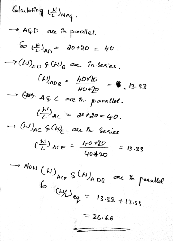
with details and explanations 3. Consider the logic function Z-((A + B).D). (C.(E+F)) (5 Marks) Realize the above Boolean function using CMOS transistors. a. btain a common Euler path for both nMO...
 with details and explanations
3. Consider the logic function Z-((A + B).D). (C.(E+F)) (5 Marks) Realize the above Boolean function using CMOS transistors. a. btain a common Euler path for both nMOS and pMOS transistors and hence draw the optimized stick diagram layout. b. O (30 Marks)
3. Consider the logic function Z-((A + B).D). (C.(E+F)) (5 Marks) Realize the above Boolean function using CMOS transistors. a. btain a common Euler path for both nMOS and pMOS transistors and hence...
with details and explanations
3. Consider the logic function Z-((A + B).D). (C.(E+F)) (5 Marks) Realize the above Boolean function using CMOS transistors. a. btain a common Euler path for both nMOS and pMOS transistors and hence draw the optimized stick diagram layout. b. O (30 Marks)
3. Consider the logic function Z-((A + B).D). (C.(E+F)) (5 Marks) Realize the above Boolean function using CMOS transistors. a. btain a common Euler path for both nMOS and pMOS transistors and hence...
 Please with details and explanations
The layout of a CMOS complex logic circuit is given in the Figure 1. 4. (10 Marks) Draw the corresponding circuit diagram; and cdlculate the (equivaent of all the nMOS and PMOS transistors for simultaneous switching of all the inputs, assuming that (W/L)p = 15 for all pMOS transistors and (w/2), a. 5 for all nMOS (10 Marks) transistors Vdd PMOS IL NMOS Figure 1
The layout of a CMOS complex logic circuit is given...
Please with details and explanations
The layout of a CMOS complex logic circuit is given in the Figure 1. 4. (10 Marks) Draw the corresponding circuit diagram; and cdlculate the (equivaent of all the nMOS and PMOS transistors for simultaneous switching of all the inputs, assuming that (W/L)p = 15 for all pMOS transistors and (w/2), a. 5 for all nMOS (10 Marks) transistors Vdd PMOS IL NMOS Figure 1
The layout of a CMOS complex logic circuit is given...
 The layout of a CMOS complex logic circuit is given in the Figure 1. 4. Draw the corresponding circuit diagram; and (10 Marks) a. b. Colculate the W/Doivalent of all the nMOS and PMOS transistors for simultaneous switching of all the inputs, assuming that (W/, 25 for all MOS transistors and (W/, 20 for al nMOS transistors. (10 Marks) FIA, B,C,D,E ) A B Figure 1
The layout of a CMOS complex logic circuit is given in the Figure 1....
The layout of a CMOS complex logic circuit is given in the Figure 1. 4. Draw the corresponding circuit diagram; and (10 Marks) a. b. Colculate the W/Doivalent of all the nMOS and PMOS transistors for simultaneous switching of all the inputs, assuming that (W/, 25 for all MOS transistors and (W/, 20 for al nMOS transistors. (10 Marks) FIA, B,C,D,E ) A B Figure 1
The layout of a CMOS complex logic circuit is given in the Figure 1....
 The layout of a CMOS complex logic circuit is given in the Figure 1 4. Draw the corresponding circuit diagram; and (10 Marks) a. b. Calculate the (W) of all the nMOS and PMOS transistors for simultaneous switching (W/), 15 for all of all the inputs, assuming that (Wh),-20 for all pMOS transistors and (w/L), = 15 for all (WL 20 for all pMOS transistors and (10 Marks) nMOS transistors VDD n well metal poly silicon n+ diffussion OUT Contact...
 The layout of a CMOS complex logic circuit is given in the
Figure 1. Draw the corresponding circuit diagram; and
Calculate the (W⁄L)_equivalent of all the nMOS and PMOS
transistors for simultaneous switching of all the inputs, assuming
that (W⁄L)p =20 for all pMOS transistors and (W⁄L)n =15 for all
nMOS transistors.
Windows VDD poly silicon n+ diffussion OUT P+ diffusion Centact GND
Windows VDD poly silicon n+ diffussion OUT P+ diffusion Centact GND
The layout of a CMOS complex logic circuit is given in the
Figure 1. Draw the corresponding circuit diagram; and
Calculate the (W⁄L)_equivalent of all the nMOS and PMOS
transistors for simultaneous switching of all the inputs, assuming
that (W⁄L)p =20 for all pMOS transistors and (W⁄L)n =15 for all
nMOS transistors.
Windows VDD poly silicon n+ diffussion OUT P+ diffusion Centact GND
Windows VDD poly silicon n+ diffussion OUT P+ diffusion Centact GND
 with details and explanations
4. The layout of a CMOS complex logic circuit is eiven in the Figure 1 (10 Marks) Calculate the (/equvalent of all the nMoS and PMOS transistors for simultaneous switching of all the inputs, assuming that (W/1), 15 for all pMOS transistors and (W/L), 5 for all nMOS Draw the corresponding circuit diagram; and a. b. (10 Marks) transistors Vdd PMOS NMOS GND Figure 1
4. The layout of a CMOS complex logic circuit is eiven...
with details and explanations
4. The layout of a CMOS complex logic circuit is eiven in the Figure 1 (10 Marks) Calculate the (/equvalent of all the nMoS and PMOS transistors for simultaneous switching of all the inputs, assuming that (W/1), 15 for all pMOS transistors and (W/L), 5 for all nMOS Draw the corresponding circuit diagram; and a. b. (10 Marks) transistors Vdd PMOS NMOS GND Figure 1
4. The layout of a CMOS complex logic circuit is eiven...
 The layout of a CMOS complex logiccircuit is given in the Figure 1 4. (10 Marks) a. Draw the corresponding circuit diagram;and b. calculate the (uivains f allthe nMoS and PMOS transistors for simultaneous switching of all the inputs, assumingthat(W/15 for all pMOS transistors and 10 for all equivalent 15 for all pMOS transistors and(W/D)10for all (10 Marks) nMOS transistors. n+ diffusion p+ diffusion ■ metal OUT polysilicon GND Figure 1
The layout of a CMOS complex logiccircuit is given...
The layout of a CMOS complex logiccircuit is given in the Figure 1 4. (10 Marks) a. Draw the corresponding circuit diagram;and b. calculate the (uivains f allthe nMoS and PMOS transistors for simultaneous switching of all the inputs, assumingthat(W/15 for all pMOS transistors and 10 for all equivalent 15 for all pMOS transistors and(W/D)10for all (10 Marks) nMOS transistors. n+ diffusion p+ diffusion ■ metal OUT polysilicon GND Figure 1
The layout of a CMOS complex logiccircuit is given...
 4. The layout of a CMOS complex logic circuit is given in the Figure t n A to l nd D using (10 Marks) qulatent of all the nmos and PMos transistors for simultaneous switching of for atl noS a. Draw the corresponding circuit diagram; and b. Calculate the (WI/n cqutvatent Of l all the inputs, assuming that (/) 15 for all pMOS transistors and (W/)- a viron ne, (10 Marks) transistors and -Vdd rol pMOS NMOS s GND
4....
4. The layout of a CMOS complex logic circuit is given in the Figure t n A to l nd D using (10 Marks) qulatent of all the nmos and PMos transistors for simultaneous switching of for atl noS a. Draw the corresponding circuit diagram; and b. Calculate the (WI/n cqutvatent Of l all the inputs, assuming that (/) 15 for all pMOS transistors and (W/)- a viron ne, (10 Marks) transistors and -Vdd rol pMOS NMOS s GND
4....
 a) What is the logic function implemented by the gate on the right? b) Design the NMOS transistor network and select the device sizes for the PMOS and NMOS transistors to give a delay similar to that of the typical symmetric CMOS reference inverter (W/L-12/1,5/1]) with the same C. c) What is the equivalent W/L ratio of the PMOS switching network then all of the PMOS transistors are on? SV D Logic inputs .toF NMOS network
 3. (20 points). A CMOS logic circuit is a generalization of the CMOS inverter. CMOS employs MOS transistors of both polarities. a) In Fig. 3 indicate NMOS and PMOS transistors; b) The inverter consists of an NMOS pulldown and PMOS pull-up transistor. Draw the CMOS NOT gate. Gate Gate Oxlde Oxlde Fig.3
3. (20 points). A CMOS logic circuit is a generalization of the CMOS inverter. CMOS employs MOS transistors of both polarities. a) In Fig. 3 indicate NMOS and...
3. (20 points). A CMOS logic circuit is a generalization of the CMOS inverter. CMOS employs MOS transistors of both polarities. a) In Fig. 3 indicate NMOS and PMOS transistors; b) The inverter consists of an NMOS pulldown and PMOS pull-up transistor. Draw the CMOS NOT gate. Gate Gate Oxlde Oxlde Fig.3
3. (20 points). A CMOS logic circuit is a generalization of the CMOS inverter. CMOS employs MOS transistors of both polarities. a) In Fig. 3 indicate NMOS and...
 with details and explanations
3. Consider the logic function Z-((A + B).D). (C.(E+F)) (5 Marks) Realize the above Boolean function using CMOS transistors. a. btain a common Euler path for both nMOS and pMOS transistors and hence draw the optimized stick diagram layout. b. O (30 Marks)
3. Consider the logic function Z-((A + B).D). (C.(E+F)) (5 Marks) Realize the above Boolean function using CMOS transistors. a. btain a common Euler path for both nMOS and pMOS transistors and hence...
with details and explanations
3. Consider the logic function Z-((A + B).D). (C.(E+F)) (5 Marks) Realize the above Boolean function using CMOS transistors. a. btain a common Euler path for both nMOS and pMOS transistors and hence draw the optimized stick diagram layout. b. O (30 Marks)
3. Consider the logic function Z-((A + B).D). (C.(E+F)) (5 Marks) Realize the above Boolean function using CMOS transistors. a. btain a common Euler path for both nMOS and pMOS transistors and hence...
Most questions answered within 3 hours.
-
Why do organizations decline? What steps can top
management take to halt, decline, and restore organizational...
asked 38 minutes ago -
. Suppose a discrete random variable has probability
distribution
P(x) = .2 if x = 0...
asked 24 minutes ago -
Under the influence of its drive force, a snowmobile is moving
at a constant velocity along...
asked 52 minutes ago -
What mechanisms Drive speciation??
(I.e. what was Dawins theory on the orgin of species, and how...
asked 2 hours ago -
The manager at a car assembly plant believes that the mean
assembly time for a car...
asked 3 hours ago -
Which of the following is true of electron capture?
A) It decreases the nuclide's mass number...
asked 4 hours ago -
Assuming an efficiency of 43.10%, calculate the actual yield of
magnesium nitrate formed from 114.9 g...
asked 5 hours ago -
The highly pathogenic bacterium Clostridium
perfringens causes gangrene, a disease that results in the
destruction of...
asked 7 hours ago -
In the context of situation analysis, which of the following is
a category for analysis in...
asked 6 hours ago -
In a study of the gas phase decomposition of sulfuryl chloride
at 600 K SO2Cl2(g)SO2(g) +...
asked 7 hours ago -
75 g of 2-propanol (C3H8O) and 25 g of pentane are mixed in a
200 mL...
asked 7 hours ago -
The 2800-turn coil in a dc motor has an area per turn of 1.1 ×
10-2...
asked 7 hours ago