
Homework Answers


Add Answer to:
4. The layout of a CMOS complex logic circuit is given in the Figure t n A to l nd D using (10 Marks) qulatent of all the nmos and PMos transistors for simultaneous switching of for atl noS a. Dra...
with details and explanations 4. The layout of a CMOS complex logic circuit is eiven in the Figure 1 (10 Marks) Calculate the (/equvalent of all the nMoS and PMOS transistors for simultaneous swit...
 with details and explanations
4. The layout of a CMOS complex logic circuit is eiven in the Figure 1 (10 Marks) Calculate the (/equvalent of all the nMoS and PMOS transistors for simultaneous switching of all the inputs, assuming that (W/1), 15 for all pMOS transistors and (W/L), 5 for all nMOS Draw the corresponding circuit diagram; and a. b. (10 Marks) transistors Vdd PMOS NMOS GND Figure 1
4. The layout of a CMOS complex logic circuit is eiven...
with details and explanations
4. The layout of a CMOS complex logic circuit is eiven in the Figure 1 (10 Marks) Calculate the (/equvalent of all the nMoS and PMOS transistors for simultaneous switching of all the inputs, assuming that (W/1), 15 for all pMOS transistors and (W/L), 5 for all nMOS Draw the corresponding circuit diagram; and a. b. (10 Marks) transistors Vdd PMOS NMOS GND Figure 1
4. The layout of a CMOS complex logic circuit is eiven...
The layout of a CMOS complex logic circuit is given in the Figure 1 4. Draw the corresponding circuit diagram; and (10 Marks) a. b. Calculate the (W) of all the nMOS and PMOS transistors for simul...
 The layout of a CMOS complex logic circuit is given in the Figure 1 4. Draw the corresponding circuit diagram; and (10 Marks) a. b. Calculate the (W) of all the nMOS and PMOS transistors for simultaneous switching (W/), 15 for all of all the inputs, assuming that (Wh),-20 for all pMOS transistors and (w/L), = 15 for all (WL 20 for all pMOS transistors and (10 Marks) nMOS transistors VDD n well metal poly silicon n+ diffussion OUT Contact...
Please with details and explanations The layout of a CMOS complex logic circuit is given in the Figure 1. 4. (10 Marks) Draw the corresponding circuit diagram; and cdlculate the (equivaent of all...
 Please with details and explanations
The layout of a CMOS complex logic circuit is given in the Figure 1. 4. (10 Marks) Draw the corresponding circuit diagram; and cdlculate the (equivaent of all the nMOS and PMOS transistors for simultaneous switching of all the inputs, assuming that (W/L)p = 15 for all pMOS transistors and (w/2), a. 5 for all nMOS (10 Marks) transistors Vdd PMOS IL NMOS Figure 1
The layout of a CMOS complex logic circuit is given...
Please with details and explanations
The layout of a CMOS complex logic circuit is given in the Figure 1. 4. (10 Marks) Draw the corresponding circuit diagram; and cdlculate the (equivaent of all the nMOS and PMOS transistors for simultaneous switching of all the inputs, assuming that (W/L)p = 15 for all pMOS transistors and (w/2), a. 5 for all nMOS (10 Marks) transistors Vdd PMOS IL NMOS Figure 1
The layout of a CMOS complex logic circuit is given...
The layout of a CMOS complex logic circuit is given in the Figure 1. 4. Draw the corresponding circuit diagram; and (10 Marks) a. b. Colculate the W/Doivalent of all the nMOS and PMOS transistors...
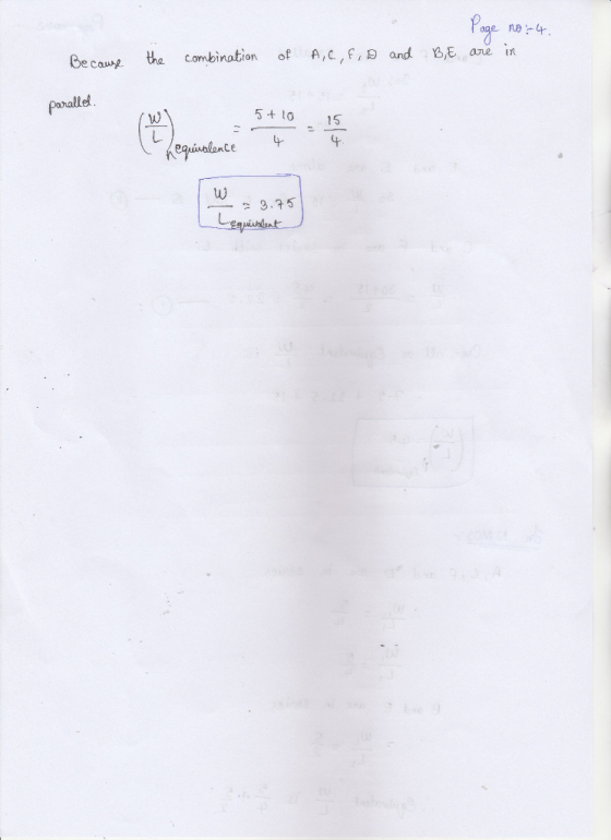
 The layout of a CMOS complex logic circuit is given in the Figure 1. 4. Draw the corresponding circuit diagram; and (10 Marks) a. b. Colculate the W/Doivalent of all the nMOS and PMOS transistors for simultaneous switching of all the inputs, assuming that (W/, 25 for all MOS transistors and (W/, 20 for al nMOS transistors. (10 Marks) FIA, B,C,D,E ) A B Figure 1
The layout of a CMOS complex logic circuit is given in the Figure 1....
The layout of a CMOS complex logic circuit is given in the Figure 1. 4. Draw the corresponding circuit diagram; and (10 Marks) a. b. Colculate the W/Doivalent of all the nMOS and PMOS transistors for simultaneous switching of all the inputs, assuming that (W/, 25 for all MOS transistors and (W/, 20 for al nMOS transistors. (10 Marks) FIA, B,C,D,E ) A B Figure 1
The layout of a CMOS complex logic circuit is given in the Figure 1....
The layout of a CMOS complex logiccircuit is given in the Figure 1 4. (10 Marks) a. Draw the corresponding circuit diagram;and b. calculate the (uivains f allthe nMoS and PMOS transistors for simulta...
 The layout of a CMOS complex logiccircuit is given in the Figure 1 4. (10 Marks) a. Draw the corresponding circuit diagram;and b. calculate the (uivains f allthe nMoS and PMOS transistors for simultaneous switching of all the inputs, assumingthat(W/15 for all pMOS transistors and 10 for all equivalent 15 for all pMOS transistors and(W/D)10for all (10 Marks) nMOS transistors. n+ diffusion p+ diffusion ■ metal OUT polysilicon GND Figure 1
The layout of a CMOS complex logiccircuit is given...
The layout of a CMOS complex logiccircuit is given in the Figure 1 4. (10 Marks) a. Draw the corresponding circuit diagram;and b. calculate the (uivains f allthe nMoS and PMOS transistors for simultaneous switching of all the inputs, assumingthat(W/15 for all pMOS transistors and 10 for all equivalent 15 for all pMOS transistors and(W/D)10for all (10 Marks) nMOS transistors. n+ diffusion p+ diffusion ■ metal OUT polysilicon GND Figure 1
The layout of a CMOS complex logiccircuit is given...
The layout of a CMOS complex logic circuit is given in the Figure 1. Draw the corresponding circuit diagram; and Calcula...
 The layout of a CMOS complex logic circuit is given in the
Figure 1. Draw the corresponding circuit diagram; and
Calculate the (W⁄L)_equivalent of all the nMOS and PMOS
transistors for simultaneous switching of all the inputs, assuming
that (W⁄L)p =20 for all pMOS transistors and (W⁄L)n =15 for all
nMOS transistors.
Windows VDD poly silicon n+ diffussion OUT P+ diffusion Centact GND
Windows VDD poly silicon n+ diffussion OUT P+ diffusion Centact GND
The layout of a CMOS complex logic circuit is given in the
Figure 1. Draw the corresponding circuit diagram; and
Calculate the (W⁄L)_equivalent of all the nMOS and PMOS
transistors for simultaneous switching of all the inputs, assuming
that (W⁄L)p =20 for all pMOS transistors and (W⁄L)n =15 for all
nMOS transistors.
Windows VDD poly silicon n+ diffussion OUT P+ diffusion Centact GND
Windows VDD poly silicon n+ diffussion OUT P+ diffusion Centact GND
The layout of a CMOS complex logic circuit is given in the Figure 1. 1. Draw the corresponding circuit diagram; and a....
 The layout of a CMOS complex logic circuit is given in the Figure 1. 1. Draw the corresponding circuit diagram; and a. b. Calculate the (W/equivaientfall the nMOS and PMOS transistors for simultaneous equivalent switching of all the inputs, assuming that (W/L), = 25 for all pMOS transistors and W-20 for all nMOS transistors F(A,B,C,D,E ) A B Figure 1
The layout of a CMOS complex logic circuit is given in the Figure 1. 1. Draw the corresponding circuit diagram;...
The layout of a CMOS complex logic circuit is given in the Figure 1. 1. Draw the corresponding circuit diagram; and a. b. Calculate the (W/equivaientfall the nMOS and PMOS transistors for simultaneous equivalent switching of all the inputs, assuming that (W/L), = 25 for all pMOS transistors and W-20 for all nMOS transistors F(A,B,C,D,E ) A B Figure 1
The layout of a CMOS complex logic circuit is given in the Figure 1. 1. Draw the corresponding circuit diagram;...
 with details and explanations
4. The layout of a CMOS complex logic circuit is eiven in the Figure 1 (10 Marks) Calculate the (/equvalent of all the nMoS and PMOS transistors for simultaneous switching of all the inputs, assuming that (W/1), 15 for all pMOS transistors and (W/L), 5 for all nMOS Draw the corresponding circuit diagram; and a. b. (10 Marks) transistors Vdd PMOS NMOS GND Figure 1
4. The layout of a CMOS complex logic circuit is eiven...
with details and explanations
4. The layout of a CMOS complex logic circuit is eiven in the Figure 1 (10 Marks) Calculate the (/equvalent of all the nMoS and PMOS transistors for simultaneous switching of all the inputs, assuming that (W/1), 15 for all pMOS transistors and (W/L), 5 for all nMOS Draw the corresponding circuit diagram; and a. b. (10 Marks) transistors Vdd PMOS NMOS GND Figure 1
4. The layout of a CMOS complex logic circuit is eiven...
 The layout of a CMOS complex logic circuit is given in the Figure 1 4. Draw the corresponding circuit diagram; and (10 Marks) a. b. Calculate the (W) of all the nMOS and PMOS transistors for simultaneous switching (W/), 15 for all of all the inputs, assuming that (Wh),-20 for all pMOS transistors and (w/L), = 15 for all (WL 20 for all pMOS transistors and (10 Marks) nMOS transistors VDD n well metal poly silicon n+ diffussion OUT Contact...
 Please with details and explanations
The layout of a CMOS complex logic circuit is given in the Figure 1. 4. (10 Marks) Draw the corresponding circuit diagram; and cdlculate the (equivaent of all the nMOS and PMOS transistors for simultaneous switching of all the inputs, assuming that (W/L)p = 15 for all pMOS transistors and (w/2), a. 5 for all nMOS (10 Marks) transistors Vdd PMOS IL NMOS Figure 1
The layout of a CMOS complex logic circuit is given...
Please with details and explanations
The layout of a CMOS complex logic circuit is given in the Figure 1. 4. (10 Marks) Draw the corresponding circuit diagram; and cdlculate the (equivaent of all the nMOS and PMOS transistors for simultaneous switching of all the inputs, assuming that (W/L)p = 15 for all pMOS transistors and (w/2), a. 5 for all nMOS (10 Marks) transistors Vdd PMOS IL NMOS Figure 1
The layout of a CMOS complex logic circuit is given...
 The layout of a CMOS complex logic circuit is given in the Figure 1. 4. Draw the corresponding circuit diagram; and (10 Marks) a. b. Colculate the W/Doivalent of all the nMOS and PMOS transistors for simultaneous switching of all the inputs, assuming that (W/, 25 for all MOS transistors and (W/, 20 for al nMOS transistors. (10 Marks) FIA, B,C,D,E ) A B Figure 1
The layout of a CMOS complex logic circuit is given in the Figure 1....
The layout of a CMOS complex logic circuit is given in the Figure 1. 4. Draw the corresponding circuit diagram; and (10 Marks) a. b. Colculate the W/Doivalent of all the nMOS and PMOS transistors for simultaneous switching of all the inputs, assuming that (W/, 25 for all MOS transistors and (W/, 20 for al nMOS transistors. (10 Marks) FIA, B,C,D,E ) A B Figure 1
The layout of a CMOS complex logic circuit is given in the Figure 1....
 The layout of a CMOS complex logiccircuit is given in the Figure 1 4. (10 Marks) a. Draw the corresponding circuit diagram;and b. calculate the (uivains f allthe nMoS and PMOS transistors for simultaneous switching of all the inputs, assumingthat(W/15 for all pMOS transistors and 10 for all equivalent 15 for all pMOS transistors and(W/D)10for all (10 Marks) nMOS transistors. n+ diffusion p+ diffusion ■ metal OUT polysilicon GND Figure 1
The layout of a CMOS complex logiccircuit is given...
The layout of a CMOS complex logiccircuit is given in the Figure 1 4. (10 Marks) a. Draw the corresponding circuit diagram;and b. calculate the (uivains f allthe nMoS and PMOS transistors for simultaneous switching of all the inputs, assumingthat(W/15 for all pMOS transistors and 10 for all equivalent 15 for all pMOS transistors and(W/D)10for all (10 Marks) nMOS transistors. n+ diffusion p+ diffusion ■ metal OUT polysilicon GND Figure 1
The layout of a CMOS complex logiccircuit is given...
 The layout of a CMOS complex logic circuit is given in the
Figure 1. Draw the corresponding circuit diagram; and
Calculate the (W⁄L)_equivalent of all the nMOS and PMOS
transistors for simultaneous switching of all the inputs, assuming
that (W⁄L)p =20 for all pMOS transistors and (W⁄L)n =15 for all
nMOS transistors.
Windows VDD poly silicon n+ diffussion OUT P+ diffusion Centact GND
Windows VDD poly silicon n+ diffussion OUT P+ diffusion Centact GND
The layout of a CMOS complex logic circuit is given in the
Figure 1. Draw the corresponding circuit diagram; and
Calculate the (W⁄L)_equivalent of all the nMOS and PMOS
transistors for simultaneous switching of all the inputs, assuming
that (W⁄L)p =20 for all pMOS transistors and (W⁄L)n =15 for all
nMOS transistors.
Windows VDD poly silicon n+ diffussion OUT P+ diffusion Centact GND
Windows VDD poly silicon n+ diffussion OUT P+ diffusion Centact GND
 The layout of a CMOS complex logic circuit is given in the Figure 1. 1. Draw the corresponding circuit diagram; and a. b. Calculate the (W/equivaientfall the nMOS and PMOS transistors for simultaneous equivalent switching of all the inputs, assuming that (W/L), = 25 for all pMOS transistors and W-20 for all nMOS transistors F(A,B,C,D,E ) A B Figure 1
The layout of a CMOS complex logic circuit is given in the Figure 1. 1. Draw the corresponding circuit diagram;...
The layout of a CMOS complex logic circuit is given in the Figure 1. 1. Draw the corresponding circuit diagram; and a. b. Calculate the (W/equivaientfall the nMOS and PMOS transistors for simultaneous equivalent switching of all the inputs, assuming that (W/L), = 25 for all pMOS transistors and W-20 for all nMOS transistors F(A,B,C,D,E ) A B Figure 1
The layout of a CMOS complex logic circuit is given in the Figure 1. 1. Draw the corresponding circuit diagram;...
Most questions answered within 3 hours.
-
A gas occupies 200. mL in a piston. If the pressure of the
piston were decreased...
asked 9 minutes ago -
A fossil is found to have a 14C level of 71.0% compared to
living organisms. How...
asked 12 minutes ago -
Many communist or socialist countries have a department that
addresses public health as well as the...
asked 14 minutes ago -
the following questions are either true or false answers
1. The Central Limit Theorem allows one...
asked 15 minutes ago -
The patient recovery time from a particular surgical procedure
is normally distributed with a mean of...
asked 21 minutes ago -
Human relations refer to the way a company arranges people,
jobs, and communications so that work...
asked 38 minutes ago -
Python Program: Design the logic for and implement a program
that merges the two files into...
asked 36 minutes ago -
The specific radiocarbon activity of a sample of wood is 6.25
gms dpm/gm of carbon. The...
asked 41 minutes ago -
An aqueous magnesium chloride solution is made by dissolving
6.96 moles of MgCl2 in sufficient water...
asked 44 minutes ago -
Ken believes the average age of men who come to get a haircut at
his barber...
asked 1 hour ago -
(Ratio Analysis): Last year Co. XYZ had sales of $ 400,000, with
“cost of goods sold”...
asked 1 hour ago -
can someone please write the balanced chemical
equation for the synthesis of Bromoacetanilide
from;
aniline +...
asked 1 hour ago