
Homework Answers
Add Answer to:
Example: CS amplifier Design the CS stage shown to the right with A-SVN, Rin-50㏀, and P diss 5mW...
4. (20 pts) - Design the CS stage below for a voltage gain of 6, an...
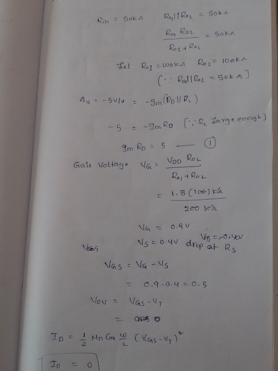
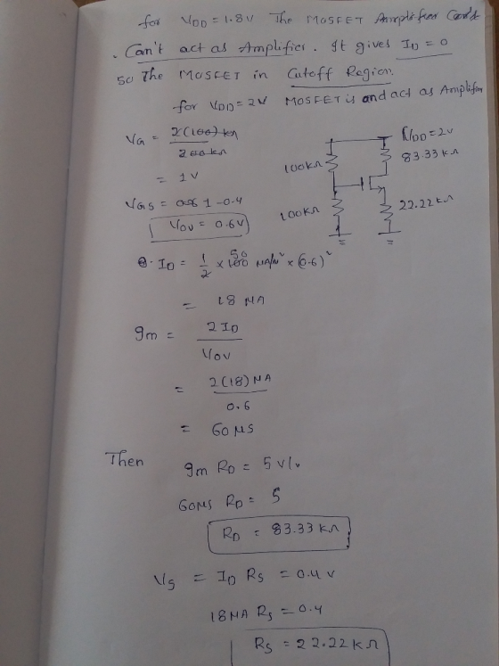
 4. (20 pts) - Design the CS stage below for a voltage gain of 6, an input impedance of 100 k12, and a power budget of 5 mW. Assume a voltage drop of 500 mV across Rs. _VoD = 2V un cox = 200MA/v2 VTH = 0.5V ovout =0 Vin Ri, Rz, Ro. Rs. Z ?
4. (20 pts) - Design the CS stage below for a voltage gain of 6, an...
 4. (20 pts) - Design the CS stage below for a voltage gain of 6, an input impedance of 100 k 2, and a power budget of 5 mW. Assume a voltage drop of 500 m V across Rs. - VDD = av Mn Cox = 200MA/v² VTH = 0.50 SR SRO +00 م Vin - Jt8 R1, R₂. Ro. Rs. We ?
Exercise 7.37: Design the bias circuit for the CS amplifier. Assume the MOSFET is specified to...
 Exercise 7.37: Design the bias circuit for the CS amplifier. Assume the MOSFET is specified to have Vt 1 V, kn = 4mA/V2 and V4 = 100 V. Neglecting the Early effect, design for ID-0.5mA, VS= 3.5 V, VD6 V and VDD 15 V. Specify the values of RD and Rs If a current of 2 μΑ is used in the voltage divider, specify the values of RG1 and RG2. Give the values of the MOSFET parameters gm and ro...
Problem 3: Design Problem On Figure P3a, you have a Common Source (CS) n-channel MOSFET amplifier....
 Problem 3: Design Problem On Figure P3a, you have a Common Source (CS) n-channel MOSFET amplifier. Notice the absence of a source resistor Rsig and load resistor R. If we know how the present amplifier (the one on Figure P3a) behaves without Rsig and RL, we can infer its behaviors if Rsig and R were to be added. design the amplifier circuit on Figure P3a, i.e., you have to find appropriate values for RGj You are to RG,, RD, and...
Vout should be a sinusoid signal of 12Vp-p Dc voltage to uA741 : +/-8.5V Please simulate...
 Vout should be a sinusoid signal of 12Vp-p
Dc voltage to uA741 : +/-8.5V
Please simulate as well
please help, im completely lost on this
this is all of the information
Experiment 5. RC Sinusoidal Oscillators PURPOSE: This laboratory provides an introduction to the background, analysis and design of sinusoidal oscillators using RC feedback networks and active devices to achieve the criteria for continuous oscillations to occur. EQUIPMENT REQUIRED : 1 Operational amplifier u.A741 1 CEU development station Resistors and...
Vout should be a sinusoid signal of 12Vp-p
Dc voltage to uA741 : +/-8.5V
Please simulate as well
please help, im completely lost on this
this is all of the information
Experiment 5. RC Sinusoidal Oscillators PURPOSE: This laboratory provides an introduction to the background, analysis and design of sinusoidal oscillators using RC feedback networks and active devices to achieve the criteria for continuous oscillations to occur. EQUIPMENT REQUIRED : 1 Operational amplifier u.A741 1 CEU development station Resistors and...
 4. (20 pts) - Design the CS stage below for a voltage gain of 6, an input impedance of 100 k12, and a power budget of 5 mW. Assume a voltage drop of 500 mV across Rs. _VoD = 2V un cox = 200MA/v2 VTH = 0.5V ovout =0 Vin Ri, Rz, Ro. Rs. Z ?
 4. (20 pts) - Design the CS stage below for a voltage gain of 6, an input impedance of 100 k 2, and a power budget of 5 mW. Assume a voltage drop of 500 m V across Rs. - VDD = av Mn Cox = 200MA/v² VTH = 0.50 SR SRO +00 م Vin - Jt8 R1, R₂. Ro. Rs. We ?
 Exercise 7.37: Design the bias circuit for the CS amplifier. Assume the MOSFET is specified to have Vt 1 V, kn = 4mA/V2 and V4 = 100 V. Neglecting the Early effect, design for ID-0.5mA, VS= 3.5 V, VD6 V and VDD 15 V. Specify the values of RD and Rs If a current of 2 μΑ is used in the voltage divider, specify the values of RG1 and RG2. Give the values of the MOSFET parameters gm and ro...
 Problem 3: Design Problem On Figure P3a, you have a Common Source (CS) n-channel MOSFET amplifier. Notice the absence of a source resistor Rsig and load resistor R. If we know how the present amplifier (the one on Figure P3a) behaves without Rsig and RL, we can infer its behaviors if Rsig and R were to be added. design the amplifier circuit on Figure P3a, i.e., you have to find appropriate values for RGj You are to RG,, RD, and...
 Vout should be a sinusoid signal of 12Vp-p
Dc voltage to uA741 : +/-8.5V
Please simulate as well
please help, im completely lost on this
this is all of the information
Experiment 5. RC Sinusoidal Oscillators PURPOSE: This laboratory provides an introduction to the background, analysis and design of sinusoidal oscillators using RC feedback networks and active devices to achieve the criteria for continuous oscillations to occur. EQUIPMENT REQUIRED : 1 Operational amplifier u.A741 1 CEU development station Resistors and...
Vout should be a sinusoid signal of 12Vp-p
Dc voltage to uA741 : +/-8.5V
Please simulate as well
please help, im completely lost on this
this is all of the information
Experiment 5. RC Sinusoidal Oscillators PURPOSE: This laboratory provides an introduction to the background, analysis and design of sinusoidal oscillators using RC feedback networks and active devices to achieve the criteria for continuous oscillations to occur. EQUIPMENT REQUIRED : 1 Operational amplifier u.A741 1 CEU development station Resistors and...
Most questions answered within 3 hours.
-
Write the ionic equations for the first stage of salts
hydrolysis.
Anion, Cation?
Na2S
NiSO4
K2SO4...
asked 7 seconds ago -
suppose there is a normally distributed population with a mean of
250 and a standard deviation...
asked 43 minutes ago -
Question Three
Suppose you as project manager are using the Waterfall
development methodology on a large...
asked 1 hour ago -
Which statement is not true about welfare in Canada?
A.Benefits typically vary based on one's ability...
asked 2 hours ago -
Please help me with FLOWCHART and UML diagram for class,
thank you!
#include <iostream>
#include <fstream>...
asked 2 hours ago -
3. Describe the “logic circuit” of the Lac operon. Which
proteins are bound or not to...
asked 3 hours ago -
Ayesha’s adjusted gross income is $60,000 in 2019. She donated a
piece of artwork with a...
asked 3 hours ago -
For Dijkstra’s shortest path algorithm:
a. Give the Big-O time for Dijkstra’s shortest path algorithm
and...
asked 3 hours ago -
Phosphorus violates the 'octet rule' in biological molecules,
forming more covalent bonds than expected based on...
asked 3 hours ago -
A 1.3 eV electron has a 10-4 probability of tunneling
through a 2.4 eV potential barrier....
asked 3 hours ago -
What is the one ingredient that is common to being successful
with all stakeholders?
profit
trust...
asked 3 hours ago -
Write an assembly language 32 bit program that reads in lines of
text by a .txt...
asked 3 hours ago